 Loading…

Operating instructions Modbus
>pDRIVE< ecoMX 4V
>pDRIVE< proMX 4V
>pDRIVE< proMX 6V
>pDRIVE< multi-ecoMX
>pDRIVE<
>pDRIVE< multi-proMX
Modbus

General remarks
The following symbols should assist you in handling the instructions:
Advice, tip !
General information, note exactly !
The requirements for successful commissioning are correct selection of the device, proper planning and installation. If you have
any further questions, please contact the supplier of the device.
Capacitor discharge !
Before performing any work on or in the device, disconnect it from the mains and wait at least 15 minutes until the capacitors have
been fully discharged to ensure that there is no voltage on the device.
Automatic restart !
With certain parameter settings it may happen that the frequency inverter restarts automatically when the mains supply returns
after a power failure. Make sure that in this case neither persons nor equipment is in danger.
Commissioning and service !
Work on or in the device must be done only by duly qualified staff and in full compliance with the appropriate instructions and
pertinent regulations. In case of a fault contacts which are normally potential-free and/or PCBs may carry dangerous voltages. To
avoid any risk to humans, obey the regulations concerning «Work on Live Equipment» explicitly.
Terms of delivery
The latest edition «General Terms of Delivery of the Austrian Electrical and Electronics Industry Association» form the basis of our
deliveries and services.
Specifications in this instructions
We are always anxious to improve our products and adapt them to the latest state of the art. Therefore, we reserve the right to
modify the specifications given in this instructions at any time, particular those referring to measures and dimensions. All planning
recommendations and connection examples are non-binding suggestions for which we cannot assume liability, particularly
because the regulations to be complied depend on the type and place of installation and on the use of the devices.
Regulations
The user is responsible to ensure that the device and its components are used in compliance with the applicable regulations. It is
not permitted to use these devices in residential environments without special measures to suppress radio frequency
interferences.
Trademark rights
Please note that we do not guarantee that the connections, devices and processes described herein are free from patent or
trademark rights of third parties.

8 P01 034.00/00 HALS
Option Modbus for the frequency inverters
>pDRIVE< MX eco
This instructions describe the functions software version APSeco_A04_16 and higher
Theme Page
Modbus……………………………………………………………. 3
Function Modbus………………………………………………………..4
Hardware ………………………………………………………….9
Process data area……………………………………………. 15
Process data area……………………………………………………..16
Control word…………………………………………………………….18
Main reference value (Auxiliary reference values) ………….25
Status word ……………………………………………………………..26
Main actual value (Auxiliary actual values) ……………………29
Parameterization……………………………………………… 31
General ……………………………………………………………………32
Inverter settings ……………………………………………….39
Bus — Diagnostics…………………………………………….. 51
Diagnostics of the control / status word ………………………52
Diagnostics of the «Bus raw data» ………………………………53
Application examples ……………………………………….55
General ……………………………………………………………………56
Appendix………………………………………………………… 59
Parameter list of the >pDRIVE< MX eco……………………60
Inverter messages …………………………………………………….81
The instructions in hand cover the topics operation, parameterization and diagnostics of the >pDRIVE<
MX eco Modbus interface. Moreover, the principles of the Modbus architecture and their main
components are explained in detail.
Use this instructions additionally to the device documentation «Description of functions» and
«Mounting instructions».
In order to address an inverter via fieldbus also during mains cut-off (line contactor control,
disconnecting switch, …) the >pDRIVE< MX eco has to be supplied with an external 24 V buffer
voltage.
When using the Modbus interface only connect pins 4, 5 and 8 in order to avoid malfunction or
damage of the >pDRIVE< MX eco !
1

8 P01 034.00/00 HALS
2

Modbus
8 P01 034.00/00 HALS
3

Function Modbus
All frequency inverters of the >pDRIVE< MX eco range support the fieldbus system Modbus as standard. It is
coupled at the RJ45 socket next to the terminals (see chapter «Modbus connection», page 10).
In the Modbus network the frequency inverter is operated as slave. The used profile is designed on the basis of
the Profidrive profile VDI/VDE 3689.
Principle function
The data transfer in a Modbus network takes place via the serial device interface (RS485 2-wire) with a
master/slave method.
Only the Modbus master can send commands (request) to the other bus subscribers. Depending on the
command, the reaction (response) of the individual slave devices is either to send the desired data or to
confirm the execution of the desired operation function. During transfer of the data, request and response
constantly alternate.
The master sends commands to the slave device. This slave sends data only when prompted to do so by the
master device. The data exchange thus follows a fixed scheme. The sequence is always seen from the
viewpoint of the Modbus master.
The commands are embedded in the transferred data frame in the form of function codes. The request of the
master contains a function code that represents a command to be executed for the slave device. In the
process, the transferred data bytes contain all information required for the execution of the command. The
error check bytes enable the slave unit to check the integrity of the data received. The response of the slave
device contains the function code of the request as an «echo.»
The data bytes of the response (slave to master) depend on the function code used and are provided by the
slave device. The error check bytes enable the master to check the validity of the received data.
The structure of the sent data is defined in various Modbus protocols.
In addition to the Modbus RTU (master/slave communication in binary code) there are also the formats
Modbus-ASCII and Modbus-PLUS.
The >pDRIVE< MX eco devices support the Modbus RTU protocol.
Structure of the telegram
The telegram structure of a Modbus frame always consists of the address of the slave being addressed, the
desired request code, a data field of variable length and a 16-bit CRC to guarantee data consistency.
The end of the telegram is recognized by a pause ≥ 3.5 bytes. The structure of a byte can be set using
parameter D6.12 «Modbus format».
The transfer of the telegrams takes place according to the master/slave system through the entry of the
desired slave address in confirmed form. If a value of zero is used as the slave address, the telegram applies
for all slaves (broadcast service).
The permissible address range of the individual slaves is 1…247. There may not be two or more devices with
the same address at the bus.
To set up a single-point connection (network consists of only one master and one slave), the master
can use the address 248. When using this address, the slave
which is set by D6.10.
responds independent of its address
8 P01 034.00/00 HALS
4

Slave
Request code Data CRC 16
address
1 byte 1 byte 1…126 byte 2 byte
Creating CRC 16
CRC 16 is calculated according to the following method for checking the data security:
− Initialize CRC (16-bit register) to hex FFFF
− Execution from the first to the last byte of the message:
CRC XOR <byte> → CRC
Execute (8 times)
Move CRC by 1 bit to the right
If output bit = 1, execute CRC XOR A001 hex → CRC.
End of execution
End of execution
− The CRC value which is calculated that way is initially transferred with the low-order byte and then with
the high-order byte.
Modbus functions / request code
Request code
8 P01 034.00/00 HALS
hex
03 hex Read Holding Registers No
06 hex Write Single Register Yes
08 hex Diagnostics No
17 hex Read/write multiple reg. No
Modbus function Broadcast Description Use
Reading of a single parameter
(16 bit) or a maximum of 63
parameters with consecutive
logical address
Writing of a single parameter
(16 bit)
Service for fieldbus diagnostics
(requests with subcodes)
Request for writing and reading
several words with consecutive
logical addresses
Parameterization,
Process data
ZTW + IW
Parameterization
Diagnostics
Process data
STW+SW,
ZTW + IW
Structure of the Modbus user data
The available request codes of the Modbus provide services for various tasks.
Diagnostic functions (request code hex 08)
Using the request code 08 hex and its subcodes, bus-specific information can be read in order to evaluate the
quality of transmission statistically.
5

Request telegram Master → >pDRIVE< MX eco
Slave
address
Request Subcode Request data CRC 16
08 hex Hi Lo Hi Lo Lo Hi
1 byte 1 byte 2 bytes 2 bytes 2 bytes
Response telegram >pDRIVE< MX eco → Master
Slave
address
Response Subcode Response data CRC 16
08 hex Hi Lo Hi Lo Lo Hi
1 byte 1 byte 2 bytes 2 bytes 2 bytes
Subcode Request data Response data Description
00 XX YY XX YY The request causes an echo at the respective slave.
The response telegram of the slave is a copy of the
request telegram.
0A 00 00 00 00 Reset counter
0C 00 00 = actual value of the
counter
0E 00 00 = actual value of the
counter
Reading out the CRC Error Message counter
(number of the faulty received telegrams)
Reading out the telegram counter
(number of the telegrams received from the slave,
independent of the type of telegram)
Parameterization of the >pDRIVE< MX eco (request code hex 03, 06)
By means of the services Read (03 hex) and Write (06 hex) of parameters all inverter-internal parameters can
be accessed via their logical address.
For details, see chapter «Parameterization», page 31.
Monitoring and control of the >pDRIVE< MX eco (request codes hex 03, 17)
By means of the services Read (03 hex) and Write/Read (17 hex) of multiple registers access to device-internal
addresses of the control word and status word as well as to the available reference values and actual values is
possible.
Therewith pure monitoring as well as complete control of the >pDRIVE< MX eco is possible. The deviceinternal drive profile is designed on the basis of the Profidrive profile (VDI/VDE 3689).
Unlike the telegram structure predefined by the Profidrive profile (PPO types 1…5), the lengths of the telegrams
can be freely defined for both directions (master → slave / slave → master) in Modbus. As a result the telegram
length can be optimized according to the existing requirements of the process.
Example of a Modbus user data telegram
8 P01 034.00/00 HALS
6

Master → >pDRIVE< MX eco
For control of the >pDRIVE< MX eco the addresses 51D…526 hex are used. The number of the inverter-internal
and actually used reference values can be preset by means of parameter D6.100 «No. of Bus-ref. values». The
reference values are configured by means of parameters D6.101…D6.133.
Word PZD1 PZD2 PZD3 PZD4 PZD5 PZD6 PZD7 PZD8 PZD9 PZD10
User data STW SW 1 SW 2 SW 3 SW 4 SW 5 SW 6 SW 7 SW 8 SW 9
Log. address (hex) 51D 51E 51F 520 521 522 523 524 525 526
Configuration — D6.101 D6.105 D6.109 D6.113 D6.117 D6.121 D6.125 D6.129 D6.133
PZD … Process data word
STW … Control word, 16 bit chain of commands. (11 bits corresponding to Profidrive profile, 5 bits freely
usable)
-14
SW … Reference value, 16 bit display, -200…+200 %, resolution 2
>pDRIVE< MX eco → Master
The addresses FA…103 hex are used to read out information provided by the >pDRIVE< MX eco like status
word and actual values. The number of the inverter-internal and actually handled actual values can be preset
by means of parameter D6.137 «Number actual values». The actual values are configured by means of
parameters D6.138…D6.170.
Word PZD1 PZD2 PZD3 PZD4 PZD5 PZD6 PZD7 PZD8 PZD9 PZD10
User data ZTW IW 1 IW 2 IW 3 IW 4 IW 5 IW 6 IW 7 IW 8 IW 9
Log. address (hex) FA FB FC FD FE FF 100 101 102 103
Configuration D6.138 D6.142 D6.146 D6.150 D6.154 D6.158 D6.162 D6.166 D6.170
PZD … Process data word
ZTW … Status word, 16 bit chain of commands. (11 bits corresponding to Profidrive profile, 5 bits freely
usable)
8 P01 034.00/00 HALS
IW … Actual value, 16 bit display, -200…+200 %, resolution 2-14
A detailed description of the control word and status word can be found in chapter «Process data
area», page 16.
7

Structure of the network
The typical Modbus topology corresponds to an RS485 2-wire serial bus network with drop lines. The
individual subscribers are connected using a 2-wire, screened twisted cable (typ. Cat 5), whereby only the
signals D1, D2 and Common are connected.
According to the Modbus recommendations, both bus lines are to be connected with one 650 Ω resistor
against 5 V and ground when installing the master. At both ends of the bus segment, the bus cable is to be
terminated with a 120 Ω resistor and a serially connected 1 nF capacitor.
At every bus segment, a maximum of 32 subscribers (including repeater) can be operated. The maximum line
extension amounts to 1000 m at 19.2 kBaud. Principally, the drop lines must be kept as short as possible
(max.. 20 m for a single line, 40 m in total in case of centralized distribution).
Technical key data of a Modbus network
Maximum number of subscribers: 247 in all segments
Maximum number of subscribers per segment: 32 including the repeater
Bus cable: Screened, 2 x twisted, two-wire line
Characteristic impedance:
Distributed capacitance:
Loop resistance:
Wire cross-section:
100…120 Ω
< 60 nF/km
< 160 Ω/km
> 0.22 mm
2
Bus connection: RJ45 — screened, pin assignment 4, 5, 8
Bus termination: Every bus segment has to be terminated using a serial
connection of R = 120 Ω and C = 1 nF.
Galvanic isolation: No
Detailed information regarding the Modbus specification can also be found under www.modbus.org
(Modbus_over_serial_line_V1.pdf Edition 2002).
8 P01 034.00/00 HALS
8

Hardware
8 P01 034.00/00 HALS
9

Modbus connection
Plug assignment
Pin assignment of the RJ45 device interface
Pin Signal
Socket
*) CANopen signals
**) Supply voltage for the Matrix 3 interface converter RS232/485 (8 P01 124)
The RJ45 socket (in the duct next to the control terminals) can be used as serial interface for the fieldbus
systems Modbus and CANopen as well as to couple the PC software Matrix 3. When building up a Modbus
network, only the signals of pins 4, 5 and 8 may be used.
1 CAN_H *)
2 CAN_L *)
3 CAN_GND *)
4 D1
5 D0
6 Not used
7 VP **)
8 Common *)
8 P01 034.00/00 HALS
10

Consequently, connection is possible in two different ways:
1. Using the optional Modbus T-adapter
The Modbus T-adapter provides two RJ45 sockets for further bus wiring. On both
sockets, which are connected in parallel, only pins 4, 5 and 8 are connected so that
also pre-assembled cables (1:1 connection) can be used.
The Modbus T-adapter is available in two different lengths.
8 P01 300 Modbus T-adapter with 0.3 m connecting cable
8 P01 301 Modbus T-adapter with 1 m connecting cable
Example of a bus structure with T-adapter:
2. Using the optional Modbus splitter or an external junction box
When no Modbus T-adapter is used, please ensure that only the three pins
4, 5 and 8 at the RJ45 connector of the bus connection are connected.
Using the PHOENIX CONTACT VARIOSUB RJ45 QUICKON connector is a
8 P01 034.00/00 HALS
simple and capable solution to establish a connection between the bus
subscriber and the Modbus splitter.
8 P01 303 Passive Modbus splitter
8 P01 306 RJ45 Connector VARIOSUB RJ45 QUICKON
11

Example of a bus structure with Modbus splitter:
>pDRIVE< MX Modbus options
Option >pDRIVE< MODBUS T-ADAP 03 8 P01 300
Option >pDRIVE< MODBUS T-ADAP 10 8 P01 301
Option >pDRIVE< MODBUS R+C 8 P01 302
Option >pDRIVE< MODBUS SPLITTER 8 P01 303
Option >pDRIVE< RS232/485 8 P01 304
Option >pDRIVE< MODBUS PLUG 8 P01 305
Option >pDRIVE< CABLE 3-BE 8 P01 122
Option >pDRIVE< CABLE 10-BE 8 P01 123
Further recommended Modbus components
Cable LAPPKABEL, UNITRONIC® BUS FD P LD, 2×2 x0.22
When using the Modbus interface only connect pins 4, 5 and 8 in order to avoid malfunction or
damage of the >pDRIVE< MX eco !
8 P01 034.00/00 HALS
12

LED — Indicator lamps
Typically the diagnostics of the Modbus connection is executed by means of the matrix operating panel BE11.
If no operating panel is available, the actual bus state can be read out also using the built-in LED keypad.
LED Modbus state Bus state
dark
flashing
8 P01 034.00/00 HALS
LED
Local Bus
Active control source
(matrix field E4)
0 0 Terminal operation
1 0 Panel mode
0 1 Fieldbus
Modbus is not connected or inactive
LED flashes proportional to the number of the incoming and outgoing telegrams
13

8 P01 034.00/00 HALS
14

Process data area
8 P01 034.00/00 HALS
15

Process data area
The exchange of process data takes place using the Modbus request telegram code 17 hex. Therefor the
status word with 1…9 actual values is sent as a response telegram to the master when the inverter receives a
data telegram (consisting of the control word and 1…9 reference values). Typically, these telegrams are sent by
the master cyclically to the individual slaves. The achievable cycle time depends on the bus structure, the
number of bus subscribers and the transmission rate. Inside the inverter, the data are processed in a
background task (typically 10…50 ms).
Example of a process data telegram to the slave with address 10
Read process data: Status word + 6 actual values, log. address of ZTW 250 dec = 00FA hex
Write process data: Control word + 1 reference value, log. address of STW 1309 dec = 051D hex
STW= 047F, SW=4000 hex (100 %)
Request telegram Master → >pDRIVE< MX eco
Slave
address
Request Start address
«read»
(ZTW)
Number of
words to be read
(ZTW +IW)
Start address
«write»
(STW)
Number of words to
be written
(STW + SW)
— — —
17 hex Hi Lo Hi Lo Hi Lo Hi Lo — — —
1 byte 1 byte 2 bytes 2 bytes 2 bytes 2 bytes
— — — Number of
Word 1 — — — Word X CRC 16
«write»
bytes
— — — Hi Lo — — — Hi Lo Lo Hi
1 byte 2 bytes 2 bytes 2 bytes
Summary of the request telegram
Slave Code ZTW
address
0A 17 00 FA 00 07 05 1D 00 02 04 04 7F 40 00 39 A3
Number of
parameters
STW address Number of
parameters
Number
of
bytes
Word 1 Word 2 CRC *)
*) Calculation of the CRC algorithm, see chapter «Structure of the telegram», page 4.
8 P01 034.00/00 HALS
16

Response telegram >pDRIVE< MX eco → Master
Slave address
Respon
se
Number of
read bytes
Word 1 — — — Word X CRC 16
17 hex Hi Lo — — — Hi Lo Lo Hi
1 byte 1 byte 1 byte 2 bytes 2 bytes 2 bytes
Summary of the response telegram
Slave Code Number of
bytes
0A 17 0E 01 B7 40 00 20 00 20 00 20 00 — — —
— — — Word 6 Word 7 CRC
— — — 00 00 00 00 Lo Hi
Word 1 Word 2 Word 3 Word 4 Word 5 — — —
ZTW = 01B7
ITW 1 = 4000hex (f act 100%)
ITW 2 = 4000hex (P act 50%)
ITW 3 = 4000hex (T act 50%)
ITW 4 = 4000hex (I act 50%)
ITW 5 = 0000hex (no alarm)
ITW 6 = 0000hex (no fault)
If the Modbus should be used only for monitoring purposes, the «Read Holding Registers» (Multiple
Read) code 03 hex telegram should be used.
8 P01 034.00/00 HALS
In special cases, the individual access to the respective elements of the
commands 03 hex, 06 hex, and 10 hex.
process data is possible using
The design of the device-internal drive profile is based on the Profidrive profile (VDI/VDE 3689). The
standardized information of the control and status word (bits 0…10) require no further inverter-internal settings.
The reference use, the assignment of actual values and the use of the free bits (11…15) must be adjusted
accordingly in matrix field «D6 Fieldbus».
Also see chapter «Structure of the Modbus user data», page 5.
17

Control word
Assignment
Bit 15
Bit 14 5 freely configurable
Bit 13 control bits for internal or external
Bit 12 frequency inverter commands
Bit 11
Bit 10 Control O.K. No control
Bit 9 – –
Bit 8 – –
Bit 7 Reset –
Bit 6 Release reference value Lock reference value
Bit 5 Release ramp integrator Lock ramp integrator
Bit 4 Release ramp output Lock ramp output
Bit 3 Release operation Lock operation
Bit 2 Operating condition OFF 3 (Fast stop)
Bit 1 Operating condition OFF 2 (Impulse inhibit)
Bit 0 On OFF 1
High = 1 Low = 0
8 P01 034.00/00 HALS
18

Description of control word bits
Bit Value Meaning Note
0 1 ON
0 OFF 1
1 1 Operating condition
0 OFF 2
(Impulse inhibit)
2 1 Operating condition
0 OFF 3
8 P01 034.00/00 HALS
− Is accepted when the drive state is «1 .. Ready to switch on» and
changes to drive state «3 Ready to run» if the DC link is
charged.
− At active line contactor control: Change to drive state
«2 .. Charge DC link«, after successful charging the drive state
changes to «3 .. Ready to run«.
− When the command has been accepted, the drive state changes
to «13 .. OFF 1 active» and thus the drive is shut down along the
deceleration ramp.
− When the output frequency reaches zero Hz: the drive state
changes from «0 .. Not ready to switch on» to «1 .. Ready to
switch on» if the basic state (bit 1 = 0, bit 2 = 1, bit 3 = 1 and bit
10 = 1) is present.
− If a renewed OFF 1 (On) command occurs during deceleration,
the inverter tries to reach the given reference value along the
acceleration ramp. Thereby the drive state changes to «7 .. Run«.
− At active line contactor control, the line contactor is switched off
if the drive state changes to «1 .. Ready to switch on«.
«OFF 2» command canceled
− When the command has been accepted, the inverter will be
locked and the drive state changes to «19 .. Lock switching-on«.
− At active line contactor control the main contactor is switched
off.
− If the basic state (bit 1 = 0, bit 2 = 1, bit 3 = 1 and bit 10 = 1) is
given, the drive state changes to «1 .. Ready to switch on«.
The OFF 2 command can also be triggered by means of the
terminal function Impulse enable !
«OFF 3» command canceled
− When the command has been accepted, the drive state changes
to «14 .. OFF 3 active» and the drive is shut down as quickly as
possible with maximum current and maximum DC link voltage.
− When the output frequency reaches zero Hz, the drive state
changes to «19 .. Lock switching-on«.
− Thereby, at active line contactor control the main contactor is
switched off. If the OFF 3 command (bit 2 = 1) is canceled during
deceleration, fast stop is executed all the same.
19

Bit Value Meaning Note
3 1 Operation released When the command has been accepted, the inverter is released (Impulse
enable) in drive state «3 .. Ready to run» and afterwards the drive state
changes to «4 .. Operation released«.
0 Lock operation
− When the command has been accepted, the inverter will be locked
and the drive state changes to «3 .. Ready to run«.
− If the drive state is «13 .. OFF 1 active«, the inverter will be locked and
the drive state changes to «0 .. Not ready to switch on«.
− Thereby, at active line contactor control the main contactor is
switched off.
− If the basic state (bit 1 = 0, bit 2 = 1, bit 3 = 1 and bit 10 = 1) is given,
the drive state changes to «1 .. Ready to switch on«.
− If the drive state is «14 .. OFF 3 active«, the procedure is executed all
the same !
4 1 Release ramp output
Drive state «5 .. Ramp output released»
0 Lock ramp output When the command has been accepted, the output of the ramp function
generator is set to zero. The drive stops with maximum current and
maximum DC link voltage.
The drive state changes to «4 .. Operation released«.
5 1 Release ramp
Drive state «6 .. Ramp output released»
integrator
0 Stop ramp integrator When the command has been accepted, the output of the ramp function
generator is set to zero. The drive stops with maximum current and
maximum DC link voltage.
The drive state changes to «4 .. Operation released«.
6 1 Release reference
value
When the command has been accepted, the given reference value at the
input of the ramp function generator is released. The drive state changes
to «7 .. Run«.
0 Lock reference value When the command has been accepted, the input of the ramp function
generator is set to zero. As a result the drive decelerates along the set
ramp.
The drive state changes to «6 .. Ramp released«.
7 1 Reset
− The reset command is accepted at the positive edge when the drive
state is «20 .. Fault«.
− If there is no fault anymore, the drive state changes to «19 .. Lock
switching-on».
− If a fault is still remaining the drive state is furthermore «20 .. Fault«.
The reset command can also be triggered by means of the terminal
function «Ext. reset» as well as by means of the Stop/Reset key on the
keypad.
0 no meaning
8 P01 034.00/00 HALS
20

Bit Value Meaning Note
8 1 Jog 1 start Command not provided
0 Jog 1 off Command not provided
9 1 Jog 2 start Command not provided
0 Jog 2 off Command not provided
10 1 Control O.K. When the command has been accepted, the DP slave is controlled
via the bus interface. The process data become valid.
This bit must be set in order to accept control commands and/or
the free bits as well as analog signals !
0 No control
− When the command has been accepted, all data are processed
depending in status bit 9 «Control requested«. Control requested
== 1 → Behaviour according to bus fault
− If the DP slave requests control furthermore, the frequency
inverter switches over to fault state with the fault message
BUS_COMM2 (depending on the setting of parameter D6.03
«Bus error behaviour»).
In this case an alarm message is always set !
Control requested == 0 → Data to 0 ! → only I/O or panel
operation
8 P01 034.00/00 HALS
21

Summary of the most important control commands
Function
ON
Start with controlled
acceleration
OFF 1
Stop according to the set
deceleration ramp
OFF 2
Impulse inhibit
(free-wheeling)
OFF 3
Emergency stop
(deceleration at current or DC
link voltage limit)
Binary Hexadecimal
0000010001111111
Control word
47F
0000010001111110
corresponds with the
«basic state»
47E
0000010001111101
results in drive state
Lock switching-on !
47D
0000010001111011
results in drive state
Lock switching-on !
47B
Reset
Use of a free bit (e.g. 13)
during operation
Canceling
«Lock switching-on»
Basic state
start command
xxxxx1xx1xxxxxxx
0000010001111111
+0010000000000000
0010010001111111
«15 Lock switching-on»
0000010001111110
0000010001111111
e.g. 480
47F
+2000
247F
8 P01 034.00/00 HALS
e.g.:
47E
47F
22

Simplified state machine
For standard control with the commands:
− Start / Stop along the inverter-internal acceleration / deceleration ramps
− Impulse inhibit
− Emergency stop
− Reset of a fault
8 P01 034.00/00 HALS
The commands Impulse inhibit (OFF 2), Fast stop (OFF 3) as well as a fault which has been reset
always result in drive state «Lock switching-on» !
In order to reach drive state «Run» it is necessary to send the basic state (bit 0 = 0, bit 1, 2 = 1) before
transmitting the start command (bit 0 = 1).
After connecting the mains (bootup of the drive) the basic state (bit 0 = 0, bit 1, 2 =1) must be provided
in order to reach drive state «Ready to switch on».
23

State machine Profidrive
Bootup
Not ready to switch on
0
Control OK +
OFF1 + basic state
Ready to switch on
1
ON
Charge DC link
2
Hardware Ready
Ready to run
3
Hardware
Not Ready
Lock operation
OFF 1
ON after OFF1
19
13
On +
released
Lock switching-on
Lock
operation
fis0
OFF 1 active
OFF 1
fis0
OFF 3 active
14
OFF 3
OFF 2
No
fault
20
Fault
Fault
All states
also OFF 3!
Release operation
4
Operation released
Release ramp output
5
Ramp output released
Release ramp
6
Ramp released
Release SW Lock SW
Run
7
Ramp hold
Lock operation
Lock
ramp output
8 P01 034.00/00 HALS
Top priorityLowest priority
24

Main reference value (Auxiliary reference values)
Depending on the setting of parameter D6.100 «No. of Bus-ref. values», 1…9 reference values are available in
the Modbus user data protocol. The meaning of the individual reference value words (16 bits each) is defined
by parameterization of the >pDRIVE< MX eco using the Matrix surface.
The reference values can be divided into two groups:
− inverter-internal reference values like e.g. f-reference, PID actual/reference value and suchlike (according
to the reference use)
− forwarding to the analog outputs for external use, without influencing the inverter control (bit 10 STW
must be 1 !).
The reference values are linear scaled values with 16 bit display.
That is: 0 % = 0 (0 hex), 100 % = 214 (4000 hex)
-14
Therefrom a presentable data range of -200…+200 % with a resolution of 2
% Binary Hexadecimal Decimal
199.9939 01111111 11111111 7FFF 32767
100.0000 01000000 00000000 4000 16384
0.0061 00000000 00000001 0001 1
0.0000 00000000 00000000 0000 0
-0.0061 11111111 11111111 FFFF -1
-100.0000 11000000 00000000 C000 -16384
-200.0000 10000000 00000000 8000 -32768
The reference values are scaled by means of parameterization in matrix field D6. All reference values are
scaled in Hz or %.
(0.0061 %) results.
Using bits 11…15 of the control word
8 P01 034.00/00 HALS
According to the Profibus profile bits 11…15 are not defined and therefore they can be freely used by the user.
When the frequency inverter is parameterized appropriate, this digital information can be used
− for inverter-internal control signals (corresponding to the use of the digital inputs) or
− totally separated from the inverter functions in order to transmit information using the digital outputs of
the frequency inverter (bit 10 STW must be 1 !).
This additional information (bit 11…15) are added to the control word in the corresponding numerical format.
Use Free control bits Possible reference values
Inverter – «internal» f-reference 2
2nd ramp
External fault
PID active
Mains ON(OFF)
f-reference 1
f-reference 2
f-correction
PID ref. value
PID actual value
…
(for the complete list see matrix filed D6)
Inverter – «external» Relay and digital outputs of the basic card
or the option card IO11 or IO12
Analog output of the basic card or
the option card >pDRIVE< IO12
25
- Manuals
- Brands
- Vatech Manuals
- DC Drives
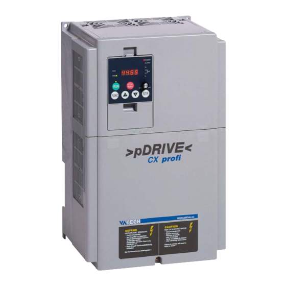
- pDRIVE CX profi
- Operating and mounting instructions manual
-
Contents
-
Table of Contents
-
Bookmarks
Quick Links
VA TECH ELIN EBG Elektronik
Operating and Mounting instructions
>pDRIVE< CX profi
The Power Drives Company
Summary of Contents for Vatech pDRIVE CX profi
-
Page 1
VA TECH ELIN EBG Elektronik Operating and Mounting instructions >pDRIVE< CX profi The Power Drives Company… -
Page 2: Parameters
Safety instructions General information, note exactly ! The requirements for a successfull commissioning are a correct selection of the unit, projection and mounting. In case of further questions, please contact the supplier or call the manufacturer of the unit directly. Capacitor discharge ! Before any work on or in the unit, disconnect from the mains and wait at least 5 minutes until the D.C.link capacitors have been fully discharged.
-
Page 3
Operating and Mounting the Frequency inverter >pDRIVE< CX profi 11…37 kW, 3 AC 380…480 V Topic Page Operating Parameters Displays Projecting Mounting Connection Options Start-up Log Appendix A This manual includes the topics operating, description of parameters and displays, projecting, mounting, connection and options. Regulations for the observance of the CE-directive and the new Power-Drive-Standard (EN 61800-3) are described in chapter “CE Marking”. -
Page 4: Displays
Operating using the control panel built-in Description of the control panel Configurable LED display RUN button starts the inverter when it POTENTIOMETER is not controlled via the to adjust the frequency. terminal strip The LED lights up as soon as the frequency can be set using the potentiometer STOP/RESET button…
-
Page 5: Mounting
Example of programming to set the frequency and to start the inverter Operating & Mounting instructions – 8 074 143.03/03 – Page 3…
-
Page 6
LEDs on the control panel Power-LED Alarm-LED RUN-LED Hz-LED PRG-LED V-LED A-LED RUN-button %-LED POTI-LED Power-LED: lights up when the inverter is connected to mains supply, that means there is a voltage. Alarm-LED: lights up in case of a trip at the inverter. Hz-LED: indicates that the value of the display shows frequency in hertz. -
Page 7
Overview of control levels Operating & Mounting instructions – 8 074 143.03/03 – Page 5… -
Page 8
Changing the indication of the LED display: 1.) Switch to the 1st user level using the FUNC button. 2.) Use the UP/DOWN buttons to select the required display. 3.) Press the STR button to confirm the selection and to return to the display level. Changing parameter settings on the 1st control level: 1.) Switch to the 1st control level using the FUNC button. -
Page 9: Parameter Name
Overview of parameters The following overviwe shows all parameters arranged according to their functions. Display actual values Factory Parameter name Adjusting range default page d001 Output frequency read only d002 Output current read only d003 Direction of rotation read only d004 PID controller feedback read only d005 Condition of digital inputs…
-
Page 10
Analog inputs Factory Parameter name Adjusting range default page A011 External frequency start O (0…10V) 0,00…400,0 Hz 0,00 Hz A101 External frequency start OI (4…20mA) 0,00…400,0 Hz 0,00 Hz A111 External frequency start O2 (-10…+10V) -400,0…+400,0 Hz 0,00 Hz A012 External frequency end O (0…10V) 0,00…400,0 Hz 0,00 Hz A102 External frequency end OI (4…20mA) -
Page 11
V/f characteristic Factory Parameter name Adjusting range default page A041 Torque boost method selection 00 or 01 A042 Manual torque boost setting 0,0…20,0 % 1,0 % A043 Manual torque boost frequency point 0,0…50,0 % 5,0 % A044 V/f characteristic setting 00 to 02 A045 Voltage gain setting 20…100 %… -
Page 12
Frequency limits Factory Parameter name Adjusting range default page A061 Frequency upper limit 0,00…400,0 Hz 0,00 Hz A062 Frequency lower limit 0,00…400,0 Hz 0,00 Hz A063 1st Jump frequency 0,00…400,0 Hz 0,00 Hz A064 1st Jump frequency width 0,00…10,0 Hz 0,50 Hz A065 2nd Jump frequency 0,00…400,0 Hz… -
Page 13
Thermal protection Factory Parameter name Adjusting range default page b012 Electronic overload setting 0,2…1,2 x I FI-I b013 Electronic overload characteristic 00 to 02 b015 Free electronic thermal: frequency 1 0…400 Hz 0 Hz b016 Free electronic thermal: current 1 0,0…1000 A 0,0 A b017… -
Page 14: Table Of Contents
Digital outputs Factory Parameter name Adjusting range default page C021 Function of relay 11 00 to 13 C022 Function of relay 12 00 to 13 C026 Function of relay AL 00 to 13 C031 Relay output 11: Inversion 00 or 01 C032 Relay output 12: Inversion 00 or 01…
-
Page 15
2nd Set Factory Parameter name Adjusting range default page A203 2nd Base frequency 30…400 Hz 50 Hz A204 2nd Maximum Frequency 30…400 Hz 50 Hz F202 2nd Acceleration ramp 0,01…3600 s 30 s F203 2nd Deceleration ramp 0,01…3600 s 30 s A220 2nd Internal pre-set speed 0,00…400,0 Hz 0,00 Hz… -
Page 16
Serial communication Factory Parameter name Adjusting range default page RS485 C070 Data command 02 to 05 C071 Transmission speed 02 to 06 C072 Identification code 1…32 C073 Data bits 7 or 8 C074 Parity 00 to 02 C075 Number of Stop bits 1 or 2 C078 Waiting time 0…1000 ms… -
Page 17
Commissioning Before working with the equipment check following points: 1.) Check that mains supply and motor cables are connected properly. 2.) Are the control lines properly connected to the right terminals ? 3.) s the frequency inverter properly grounded and assembled ? 4.) Remove installation residues, such as cable residues, in order to avoid short circuits. -
Page 18
Description of parameters The parameters of the >pDRIVE< CX are arranged and described according to their functions. The following example explains the attributes of parameters: A038 Jogging frequency 0,0…9,9 Hz 1,0 Hz Factory default Name of parameter Number of parameter Adjusting range Group of parameter Parameter description:… -
Page 19
d005 Condition of digital inputs read only Status display (ON/OFF) of digital inputs on the LED display. EIN/ON (24 V) EIN/ON (24 V) AUS/OFF (0 V) AUS/OFF (0 V) Eingangsnr.: 5 4 3 2 1 Input No.: d006 Condition of digital outputs read only Status display (ON/OFF) of digital outputs on the LED display. -
Page 20
Base settings Get Started A003 Base frequency 30…400 Hz 50 Hz Adjustment of the base frequency. The base frequency is the frequency at which the output voltage reaches its maximum value. Normally, the base frequency is equal to the nominal motor frequency. A004 Maximum frequency 30…400 Hz… -
Page 21
A001 Method of speed command 00 to 05 Setting Reference via Potentiometer on the keypad Control terminals (analog inputs or multi speeds) Parameter F001, A020/A220 or motorpotentiometer RS 485 Option 1 Option 2 A002 Method of run command 01 to 05 Setting Control command via Control terminals (FW, REV inputs) -
Page 22
A014 Analog signal reference for end O (0…10V) VIC 0…100 % 100 % A104 Analog signal ref. for end OI (4…20mA) 0…100 % 100 % A114 Analog signal ref. for end O2 (-10…+10V) -100…+100 % 100 % This parameters define the maximum reference value if it should be other than 10 V, 20 mA or +10 V. -
Page 23
A005 AT Terminal selection 00 or 01 Setting Function Switching between 0…10V and 4…20mA (O / OI) Switching between 0…10V and -10…+10V (O / O2) A006 O2 Control selection 00 to 02 Setting Function Single reference value (without f-correction) Addition of f-correction without changing direction Addition of f-correction with change of direction Parameter Terminal… -
Page 24
C081 Adjustment 0…10 V input 0…9999 Default C082 Adjustment 4…20 mA input 0…9999 Default C083 Adjustment -10…+10 V input 0…9999 Default C121 Offset-adjustment 0…10 V input 0…9999 Default C122 Offset-adjustment 4…20 mA input 0…9999 Default C123 Offset-adjustment -10…+10 V input 0…9999 This adjustments are done in factory and should not be changed! Multispeeds… -
Page 25
Multi speeds − “binary” function CF1 CF2 CF3 CF4 Adjusted value Parameter Internal preset speed if A001=02 A020 Multispeed 1 A021 Multispeed 2 A022 Multispeed 3 A023 Multispeed 4 A024 Multispeed 5 A025 Multispeed 6 A026 Multispeed 7 A027 Multispeed 8 A028 Multispeed 9 A029… -
Page 26
V/f characteristic A041 Torque boost method selection 00 or 01 Setting Function manual boost automatic boost A042 Manual torque boost setting 0,0…20,0 % 1,0 % A043 Manual torque boost frequency point 0,0…50,0 % 5,0 % For applications which require higher starting torque, the standard starting torque can be increased. Use parameter A041 to select between automatic and manual boost. -
Page 27
A045 Voltage gain setting 20…100 % 100 % The output voltage can be set within the range of 20…100 % of the motor voltage set with parameter A082. b036 Start reduced voltage selection 00 to 06 With this parameter the control time of the start voltage is set. Setting 00 ……. -
Page 28
Free adjustable V/f characteristic: DC brake Braking The frequency inverters >pDRIVE< CX profi have an adjustable DC brake. By locking a clocked DC rotor voltage onto the base of the motor, the rotor produces a braking torque that counteracts the rotation. With the help of the DC brake, braking a drive to minimum speed is possible, before the mechanical brake is activated. -
Page 29
Parameter A055 and A058 define the duration of DC injection braking. The value is set within the range from 0,1 to 60 seconds. Parameter A056 defines wheter the DC brake is active depending on time or depending on a contact. Parameter A059 defines the carrier frequency during DC braking. -
Page 30
DC brake controlled via digital input (A051=00) The DC brake is activated via a digital input (D8: C001…C005=7). Note: The DC brake causes a heating of the connected motor. Be sure that the motor does not get to warm. Operating & Mounting instructions – 8 074 143.03/03 – Page 28… -
Page 31
b090 Dynamic braking ratio 0,0…100,0 % 0,0 % Adjusting the allowed duration time of the braking resistor (only at CX profi 11 and 15). Setting 0,0 % means that the internal braking unit is not active. b095 Dynamic braking selection 00 to 02 Setting Function… -
Page 32
A063 1st Jump frequency 0,00…400,0 Hz 0,00 Hz A064 1st Jump frequency width 0,00…10,0 Hz 0,50 Hz A065 2nd Jump frequency 0,00…400,0 Hz 0,00 Hz A066 2nd Jump frequency width 0,00…10,0 Hz 0,50 Hz A067 3rd Jump frequency 0,00…400,0 Hz 0,00 Hz A068 3rd Jump frequency width… -
Page 33
PID reference value The reference value is selected using parameter A001. The following values can be used as reference source: Reference value Settings Standardization Potentiometer built-in A001 = 00 0…100 % Parameter value F001 A001 = 02 0…100 % x Parameter A075 Multispeeds A020…A035 0…100 % x Parameter A075 Analog input O (0…10 V) -
Page 34
A071 Selection of PID function: ON/OFF 00 or 01 The PID controller is activated and deactivated using parameter A071. Setting Function PID controller not active PID controller active; with digital input to setting 23 (PID enable) switch-over to manual control *) After setting the scale conversion (parameter A075) this parameters are adjusted and displayed in process sizes. -
Page 35
A075 PID controller: Scale conversion 0,01…99,99 1,00 Parameter A075 allows the setting of a conversion factor for the proper process presentation of the PID reference and actual value on the LED display. Parameters A011 (A101), A012 (A102), d004, F001 and A020…A035 are converted in accordance with the setting of A075. -
Page 36
A081 Selection of AVR function 00 to 02 Parameter A081 switches the “Automatic Voltage Regulation” for the motor on and off. Setting Function AVR function active AVR function not active AVR function not active during deceleration A082 Selection of voltage for AVR 380…480 V 400 V The nominal motor voltage (380 / 400 / 415 / 440 / 460 / 480 V) is set with parameter A082. -
Page 37
A095 Switch-over 1./2. acceleration ramp 0,00…400,0 Hz 0,00 Hz A096 Switch-over 1./2. deceleration ramp 0,00…400,0 Hz 0,00 Hz Particularly, this switch-over is used for EMERGENCY STOP functions and speed-related acceleration and deceleration times. The adjusted acceleration/deceleration time is related to the maximum frequency A004. -
Page 38
Thermal protection Electronic Overload b012 Electronic overload setting 0,2…1,2 x I FI-I A thermal motor contactor (“maximum continuous current”) can be set by entering the nominal motor current in A. Note: If the value is higher than the nominal motor current, the motor cannot be protected by an electronic motor contactor. -
Page 39
Overload protection Overload restriction b021 Selection of 1st overload restriction 00 to 02 This parameter defines when the current limitation is active. Setting Function not active during acceleration and constant speed only at constant speed Note: The overload restriction is not active during deceleration. b022 Level of 1st overload restriction 0,5…1,5 x I… -
Page 40
Digital inputs Input terminals C001 Function of input 1 01 to 39, NO C002 Function of input 2 01 to 39, NO C003 Function of input 3 01 to 39, NO C004 Function of input 4 01 to 39, NO C005 Function of input 5 01 to 39, NO… -
Page 41
Explanations of the functions for the digital inputs Start/Stop via switch contacts: When the contacts are closed, a Start command is 00 Start FWD issued in the right direction (acceleration on gradient), when open, a stop command is issued (deceleration on gradient). The simultaneous 01 Start REV closing of Start forward and Start reverse also issues a Stop command to the inverter. -
Page 42
DC brake: 07 DC brake If this command is activated, the DC brake is active. Switch-over of parameters: If this command is activated, the inverter switches over to the 2nd set of parameters. Motor data, 08 2nd Set minimum and maximum limits and the accelerati- on and deceleration times are switched over. -
Page 43
External fault: The activated command leads to immediate fault shut-down with the error message „E12 — Ext. fault“. Using this input, plant errors can be 12 Ext. fault integrated in the control of the frequency inverter. The error message cn be realised using the break or make contact (parameter C011 to C015). -
Page 44
Bypass signal: 14 Bypass signal An activation of the command leads an holding of the running motor after mains operaiton. Verriegelungszeit/ Bypaßschütz/ Cut-off time bypass contactor Motorschütz/ Motor contactor Netzschütz/ Mains contactor 0,5…1s Ausgangsfreq./ Output freq. b003 After the switch-over from bypass to inverter ope- ration, the inverter takes over the running motor after the waiting time set with parameter b003. -
Page 45
External reset: Allows you to confirm an error via the terminals. During operation, an external Reset-command stops the inverter!! The signal must not be inverted and must not be issued for more than 4 seconds. 18 External reset A permanent reset is not possible. If the inverter is running without problems, it runs to 0 Hz when an RS signal is issued! In plants, where a common reset signal is used for all devices, parameter… -
Page 46
Multispeeds (“bit”-function): The multispeeds (maximum 7) are selected using the signals SF1…SF7 according to the table: SF1 SF2 SF3 SF4 SF5 SF6 SF7 Ref. value 32 Fix 1 analog value 1 (A021) 33 Fix 2 2 (A022) 3 (A023) 34 Fix 3 4 (A024) 5 (A025) 35 Fix 4… -
Page 47
C011 Condition of input C001 00 or 01 C012 Condition of input C002 00 or 01 C013 Condition of input C003 00 or 01 C014 Condition of input C004 00 or 01 C015 Condition of input C005 00 or 01 C019 Condition of input FW 00 or 01… -
Page 48: C021 Function Of Relay
Digital outputs Output terminals C021 Function of relay 11 00 to 13 C022 Function of relay 12 00 to 13 C026 Function of relay AL 00 to 13 The programmable relay outputs (terminals 11 and 12 and also AL) can be programmed using parameters C021, C022 and C026.
-
Page 49
Funktion FA1: C021, C022 oder/or C026 = 1 Funktion FA2: C021, C022 oder/or C026 = 2 “Sollwert erreicht” / “Reference value arrival” “Frequenz überschritten” / “Frequency exceeded” 1.5 Hz 0.5 Hz C042 0.5 Hz 1.5 Hz C043 0.5 Hz 1.5 Hz Ausgangs- Output signal… -
Page 50: C032 Relay Output
Function: A A L C021, C C 022 o o r C C 026 = = 0 0 5 “Error m m essage” If one of the outputs C021 or C022 is set to position 05, an error signal is issued if an error occurs. During mains failure the error signal will continue only as long as there is still power in the inverter.
-
Page 51: C042 Arrival Signal For Acceleration
Output functions Output functions C040 Overload signal output mode 00 or 01 Setting Function Message during acceleration and constant frequency Message only at constant frequency C041 Level of overload signal 1 0…2 x I Setting the parameter within a range of 0 to 200 % with reference to the nominal current of the inverter.
-
Page 52: Sec 1,0 Sec
C061 Level of thermal motor protection 0…100 % 80 % This parameter defines the level, at which the alarm message “Temperature alarm” occurs at the digital output. If this parameter is set to 0 %, the function is not active. b034 Run/Power on time 0…9999…
-
Page 53
In the event of a low-voltage trip during operation, e.g. mains failure, the inverter switches to impulse lock. If the voltage returns within the time set with b002, the inverter can be started again. Otherwise, the unit shuts down with the message undervoltage. If parameter b001 is set to 01, the time period b003 can be set after which the frequency inverter tries to start-up again (after return of power). -
Page 54
b035 Direction restriciton (input) 00 to 02 Setting Function Forward and reverse possible Only forward possible Only reverse possible b082 Start frequency adjustment 0,10…9,99 Hz 0,50 Hz The devices start with a minimum of 0,1 Hz. The value can be increased to a maximum of 9,99 Hz in increments of 0,01 Hz. Note: The acceleration and deceleration time is shorter, if the start frequency is increased. -
Page 55
b092 Cooling fan control 00 or 01 Setting Function Fan is alway running Fan runs only during operation (after mains switch-on and after stop-command the fan still runs 5 minutes) b037 Display selection 00 to 02 This parameter must be always set to 00. Motor data Motor data H003… -
Page 56
F203 2nd Deceleration ramp 0,01…3600 s 30 s Setting of required deceleration time. The time is in reference with the range from 0 Hz to maximum frequency (parameter A204). A220 2nd Internal pre-set speed 0,00…400,0 Hz 0,00 Hz Entry of frequency reference value, if function A001 is set to position 02. Allows the entry of a minimum frequency to which the inverter runs up without selecting a digital input “CF1…CF4”… -
Page 57
A292 2nd Second acceleration ramp 0,01…3600 s 15,00 s A293 2nd Second deceleration ramp 0,01…3600 s 15,00 s A294 2nd Method of second stage selection 00 or 01 Setting Function Switch-over via an external signal on a digital input (setting: 09) Switch-over when the frequencies set at parameter A295 and A296 are reached A295 2nd Stage Acceleration change over point… -
Page 58
Analog outputs Analog output C027 Function of FM PWM output 00 to 07 C028 Function of AM analog output 00 to 07 C029 Function of AMI analog output 00 to 07 Programming the function of the analog/digital output FM and of the analog outputs AM and AMI. Setting Function Analog display of the frequency… -
Page 59
Function: Analog d d isplay o o f t t hermal u u tilization C027, C C 028 o o r C C 029 = = 0 0 6 10V or 20mA correspond with the maximum thermal utilization of the motor (in accordance with the thermal motor model: parameter b012 or b212 “Electronic overload setting”). -
Page 60
Serial communication RS485 Communications C070 Data command 02 to 05 C071 Transmission speed 02 to 06 C072 Identification code 1…32 C073 Data bits 7 or 8 C074 Parity 00 to 02 C075 Number of Stop bits 1 or 2 C078 Waiting time 0…1000 ms Parameters C070…C078 allow the configuration of the serial interface RS485. -
Page 61
Software lock, Factory default b031 Software lock 00 to 10 Locks or releases adjustment of parameters. Setting Function All parameters locked (excepted parameter b031) as long as there is a lock signal at the control terminals (set one of the parameters C001…C005 to position 15) All parameters locked (excepted parameter b031 and frequency reference value F001) as long as there is a lock signal at the control terminals (set one of the parameters C001…C005 to position 15) -
Page 62
Notes Operating & Mounting instructions – 8 074 143.03/03 – Page 60… -
Page 63
Fault memory d080 Number of trips read only Display of the number of trip messages on the LED display. d081…d086 Trip messages read only Parameters d081 to d086 display the last error messages. They show the output frequency, the motor current, operating hours of motor and inverter during fault at the display. d081 shows the last error, d082 the error before … -
Page 64
Error messages The frequency inverters have protection functions against e.g. overcurrent, overvoltage, undervoltage,… In case of a trip, the output voltage is switched off, the motor stops idle and the inverter stays in trip state until the trip is resetted. Trip Possible c c ause Remedy a a ctions… -
Page 65
Trip Possible c c ause Remedy a a ctions Trips at the current transformers Current transformer is defect Replace current transfomer Trip of calculator Electromagnetic fields, Check of possible external frequency inverter defect disturbances, contact the customer service External fault An external fault is send via a Check the reason of the trip digital input of the inverter… -
Page 66
Error messages can be removed with Reset. There are several possibilities: • Link the programmed input for short time with P24 • Press the STOP/RESET key on the keypad • Switch-off the power supply Note: An inverter which operates without any failure, will decelerate to 0 Hz if an reset signal is released !! Set parameter C102 “Reset function selection”… -
Page 67
Alarm messages The frequency inverter displays alarm messages (= H) if the parameter settings do not match. Display Meaning H001 / H201 A061 / A261 > A004 / A204 H002 / H202 A062 / A262 > A004 / A204 H004 / H204 A003 / A203 >… -
Page 68
Further displays Is displayed during initialisation, when switching on and if a reset signal is issued. Is displayed in the event of low voltage or mains failure. The waiting time for automatic restart expires. (see parameter b001 to b003) Is displayed during initialisation of parameters and indicates the initialisation version: EU … -
Page 69
Special safety instructions Short mains failure During a mains failure, the >pDRIVE< CX profi frequency inverter continues operating until the intermediate circuit voltage drops below the minimum working level (approx. 20 % below the lowest supply voltage). The time depends on the mains voltage before switching off, and on the load. If a Start command is issued, the motor runs up again as soon as the power supply returns. -
Page 70
Technical Data >pDRIVE< CX profi Power data Motor rating (recomended) 11 kW 15 kW 18,5 kW 22 kW 30 kW 37 kW Continuous output power 15,2 kVA 20,1 kVA 25,3 kVA 29,4 kVA 39,4 kVA 48,4 kVA Continuous output current 22 A 29 A 37 A 43 A… -
Page 71
General technical data Standards CE-EMC directive in connection with optinal RFI filter and under consideration of the installation remarks CE low voltage directive, UL Product standard EN 61 800-3 “Power drive system” NSR directive 73/23 EWG Vibration/ Shock 5,9 m/s² (0,6 G) 10…55 Hz (CX profi 37: 2,94 m/s² (0,3 G)) Protection class class 1 in accordance with EN 50178 Environmental class… -
Page 72
Remarks on power supply Mains impedance Virtually all frequency inverters produce harmonic oscillation when connected to the mains, which can interfere with other devices due to the voltage distortions thus caused. Please note that all converters with connected intermediate circuit voltage (diode rectifier at input) are a load on the mains supply in their total output. -
Page 73
Mains fuses and cable diameters 1.) 2.) 4.) 5.) 1.) 3.) Mains s s upply Frequency i i nverter Motor- output Pre-o o r Mains f f use Lines i i n t t he Max. C C onnec- M M otor conduit Cu c c able “inverter… -
Page 74
Remarks to the inverter output side Motor cable lengths The distances between inverter and motor indicated in the table in the chapter «CE-DR Options» must be complied with. Too long motor cables can damage the inverters! Option: AMF (output motor filter) To reduce the voltage rate of rise on the inverter output and the effects on parallel lines thus possi- ble, it is of advantage to use the AMF. -
Page 75
General Mounting Information Make sure, that the input voltage is 3 AC 380…480 V ±10 %, 50/60 Hz ±5 %. Ambient factors such as high temperatures, high humidity, dust, dirt and aggressive gases must be avoided. The inverter should be installed in a well ventilated place that is protected against direct sunlight. Install the inverter on a fire-proof, vertical wall that does not transmit vibrations. -
Page 76
Dimensions >pDRIVE< CX profi 11 and 15 with option CE-DR 400/28 without filter RFI-filter incl. line choke >50 Æ7 >50 Æ7 >pDRIVE< >pDRIVE< CX profi CX profi >pDRIVE< CX profi 18 to 30 with option CE-DR 400/56 without filter RFI-filter incl. line choke >50 >50 Æ7… -
Page 77
>pDRIVE< CX profi 37 with option CE-DR 400/68 without filter RFI-filter incl. line choke >50 >50 Æ9 Æ10 >pDRIVE< >pDRIVE< CX profi CX profi Operating & Mounting instructions – 8 074 143.03/03 – Page 75… -
Page 78
Notes Operating & Mounting instructions – 8 074 143.03/03 – Page 76… -
Page 79
Power connections For wiring the power and control terminals, the front cover must be removed. Do not apply mains power to the motor terminals U, V, W, since this can cause damage to the frequency inverter. In multimotor operation, a motor protection relay must be provided for each motor. Power connections >pDRIVE<… -
Page 80
General connecting information: 1.) Power wiring with individual wires should always be installed close to the corresponding PE conductor. 2.) Control, mains supply and motor discharge should be separated, if possible 3.) Never install control lines, mains wires or motor cable in a common cable conduit!! If control lines have Control lines to cross power… -
Page 81
Control terminals Interne Verdrahtung der Steuerklemmen / internal wiring of the control terminals Externe Verdrahtung / external wiring +10V Referenz / reference; 20 mA 1 bis/to 2kOhm 0…+10V Analogeingang / analogue input -10…+10V Analogeingang / analogue input 4..20mA Analogeingang / analogue input 4…20mA Masse / ground +24V Referenz / reference;… -
Page 82
Specification of control terminals Terminal Function Description 24V potential for digital inputs; max. load 100 mA 0V potential for digital inputs Common Common connection for digital inputs Start RL Starts the inverter in forward direction Programmable approx. 5 mA per input digital inputs The digital inputs 1…5 can be programmed with parameters C001 to C005 as follows… -
Page 83
Terminal Function Description 0…10 V Potentiometer 10V reference voltage for Voltage signal 1…2 kOhm definition of frequency reference value max. 20 mA Analog voltage input frequency ref. value 0…10V or PID controller ref. value/ act. value Analog voltage input frequency ref. value -10…+10V 4…20 mA Potentiometer… -
Page 84
Terminal Function Description Relay output Minimum: 1V DC, 1mA ohmic load: 250V AC; 5A 30V DC, 5A inductive load: 250V AC; 1A 30V DC; 1A Operation “Frequency value arrival” — signal “Frequency exceeded” — signal (C042, C043) Overload message PID deviation too high Error message “Frequency arrival”… -
Page 85
Wiring examples Manual operation via the built-in keypad Following parameters have to be changed: A001= 00 Reference value via potentiometer on the keypad A002= 02 Control commands via RUN/STOP buttons F002 = 10 s Adjust acceleration time F003 = 10 s Adjust deceleration time A004= 50 Hz Increase max. -
Page 86
Operation via analogue reference value 0…10 V Following parameters have to be changed: A001 = 01 Reference value via terminal A002 = 01 Control command via digital input F002 = 10 s Adjust acceleration time F003 = 10 s Adjust deceleration time C005 = 01 REV Start reverse on digital input 5 b080 = 180… -
Page 87
Operation via analog reference value 4…20 mA Following parameters have to be changed: A001 = 01 Reference value via control terminals A002 = 01 Control command via digital input F002 = 10 s Adjust acceleration time F003 = 10 s Adjust deceleration time C002 = 16 Switch-over to 4 .. -
Page 88
Operation via multispeeds Following parameters have to be changed: A001 = 01 Reference value via control terminals A002 = 01 Control command via digital input F002 = 10 s Adjust acceleration time F003 = 10 s Adjust deceleration time C002 = 16 AT Switch-over to 4 .. -
Page 89
Operation via integrated PID controller Setting example: flow control A flow rate control should be set up with the internal PID controller of the >pDRIVE< CX . The reference value can be set via voltage input: 0…10 V = 0…300 l/h The actual value is recorded by a data recorder 0…500 l/h = 4…20 mA. -
Page 90
Reference value: Actual value: Remark: In order to ensure a correct control process within the whole PID range, the feedback value must be able to exceed the reference value. (A deviation is absolutely necessary in order to achieve a control action !) To adjust the acutal value input (0…500 l/h) to the reference value input (0…300 l/h), it is necessary to synchronize the actual value at the current input with parameter A101…A104. -
Page 91
After setting the parameters, the inverter can be started with clockwise rotation field unsing terminal FW. The example for defining the ref. value via the analog voltage input is only one configuration example. It is also possible to define the reference value using the built-in potentiometer, using parameter F001, with the UP and DOWN buttons or using the 2nd analog input. -
Page 92
RFI-filters CE-DR All devices and equipment in electric power engineering can cause electromagnetic interference and be disturbed by electromagnetic interference. Therefore, they are subject to the provisions of the EMV directive 89/336/EEC since 1.1.1996. However, frequency inverters cannot be regarded as machines with at least one mechanically moving component. -
Page 93
Technical Data Filtertype >pDRIVE< CE-DR 400/28 CE-DR 400/56 CE-DR 400/68 for >pDRIVE< inverters CX profi 11 and 15 CX profi 18…30 CX profi 37 Mains connection Phases 3 AC 3 AC 3 AC Voltage 380…480 V ±10% 380…480 V ±10% 380…480 V ±10% Nomina current 28 A… -
Page 94
Allocation table: Inverter — Options — Motor cables — Motor Operating & Mounting instructions – 8 074 143.03/03 – Page 92… -
Page 95
Regulations To satisfy the EMC directive 89/336/EEC, the following points should be kept: 1.) Mains voltage • Voltage fluctuation ≤ ±10 % • Voltage unbalance ≤ ±3 % • Frequency variations ≤ ±5 % • Voltage distortion (THD) ≤ 10 % 2.) Wiring •… -
Page 96
Mounting and Connection CE-DR Filter >pDRIVE< CX profi Never lay control and power cables in the same cable- channel !!! Crossings have to be in a right angle !!! Lay motor cables internal close together or control cables screen them !!! Mains contactor U V W PE… -
Page 97
Once the filter has been assembled on an assembly plate, the frequency inverter is fixed using the 4 drill holes on the filter. The electric connection between the filter and the frequency inverter is then made using the cable from the filter, whereby the phase-sequence is irrelevant. The mains connection is provided at the top of the filter, on terminals L1, L2 and L3. -
Page 98
AMF 450/12 AMF 450/48 AMF 450/90 Mains voltage 3 x 380…500 V 3 x 380…500 V 3 x 380…500 V Nominal current 12 A 48 A 90 A Overload capacity 20 % for 60 s 20 % for 60 s 20 % for 60 s Losses max. -
Page 99
Remarks • The switching frequencies of >pDRIVE< CX must be set to a value of 3 kHz or less in accordance to the table “allowed cable length” • Because of the higher earth capacitances, parallel motor cables should only be used for short distances (see table “allowed cable length”) •… -
Page 100
Isolated amplifier TV5, TV6 The >pDRIVE< TV5 is an active isolating amplifier which transforms the input signal (0-10 V) to an output signal (4…20 mA). The >pDRIVE< TV6 is an active isolating amplifier which transforms the input signal (0-10 V) to an output signal (0…20 mA). -
Page 101
EMC product standard for PDS (Power-Drive-Systems) EN 61800-3 In June 1996 the product standard EN 61800-3 for frequency inverter based drives was released. It has priority over the existing general standards (generic standards). If a drive is build-in into another unit for which exists an own EMC-standard then this standard has to be considered. -
Page 102
BDM: Base-Drive-Module Basic drive unit consisting of the power part and the control electronic. i.e. frequency inverter — build-in unit CDM: Complete-Drive-Module Drive module consisting of: BDM (basic unit) and possible extensions i.e. cubicle including RFI-Filter, AMF, line contactor, …) PDS: Power-Drive-System Drive system consisting of CDM (drive module), the motor, motor cable on site controlling, mains transformer, .. -
Page 103
Domestic premises: The standard calls those establishments „first enviroment“. Drives that are connected without an intermediate transformer to the public power network supplying residential areas. The valid interference limits are very low and can only be observed by keeping all installation requirements. Industrial premises: The standard refers to such environments as “second environment”. -
Page 104
>pDRIVE< CX profi Frequency inverters Start-up Log Type: CX profi 11 CX profi 15 CX profi 18 CX profi 22 CX profi 30 CX profi 37 Serial number: Code: Customer / Company: Supplier / Company: Date of delivery: Commissioning date: Parameter adjustments F-Parameters Parameter name… -
Page 105
Parameter name Factory default Setting Page A006 O2 Control selection A011 External frequency start O (0…10V) 0,00 Hz A012 External frequency end O (0…10V) 0,00 Hz A013 Analog signal ref. for Start O (0…10V) A014 Analog signal reference for end O (0…10V) 100 % A015 External frequency start pattern O (0…10V) A016 Time constant for analog signals… -
Page 106
Parameter name Factory default Setting Page A054 DC braking: braking torque A055 DC braking: braking time 0,0 s A056 DC braking: edge/level selection A057 DC braking: braking torque (start) A058 DC braking: braking time (start) 0,0 s A059 DC braking: carrier frequency 3,0 kHz A061 Frequency upper limit 0,00 Hz… -
Page 107
Parameter name Factory default Setting Page A101 External frequency start OI (4…20mA) 0,00 Hz A102 External frequency end OI (4…20mA) 0,00 Hz A103 Analog signal ref. for Start OI (4…20mA) A104 Analog signal ref. for end OI (4…20mA) 100 % A105 Ext. -
Page 108
Parameter name Factory default Setting Page b031 Software lock b034 Run/Power on time b035 Direction restriciton (input) b036 Start reduced voltage selection b037 Display selection b080 AM analog adjustment b081 FM PWM meter adjustment b082 Start frequency adjustment 0,50 Hz b083 Carrier frequency setting 3,0 kHz… -
Page 109
C-Parameters Parameter name Factory default Setting Page C001 Function of input 1 C002 Function of input 2 C003 Function of input 3 C004 Function of input 4 C005 Function of input 5 C011 Condition of input C01 C012 Condition of input C02 C013 Condition of input C03 C014 Condition of input C04 C015 Condition of input C05… -
Page 110
Parameter name Factory default Setting Page C085 Standardization of thermistor input Default C086 AM analog offset Default C087 AMI analog adjustment C088 AMI analog offset Default C101 Reference up/down selecteion C102 Reset function selection C103 Reset restart function selection C121 Offset-adjustment 0…10 V input Default C122 Offset-adjustment 4…20 mA input Default… -
Page 111
VA TECH ELIN EBG Elektronik GmbH & Co Ruthnergasse 1 A-1210 Vienna, Austria Phone: +43/1/29191-0 Due to ongoing product modifications, data subject Telefax: +43/1/29191-15 to change without notice. http://www.pdrive.cc © VA TECH ELIN EBG Elektronik GmbH & Co, 2005 HDIA 8 074 143.03/03…
Данный инвертер используется в компрессорах фирмы HERTZ Kompressoren GmbH (Германия), модель FRC-30. Дата производства ПЧ 2007 г. Мощность преобразователя частоты 30кВт.

Пользователь жаловался на отказ работы компрессора. После выезда наших специалистов и предварительной диагностике на объекте заказчика было выявлено возникновение ошибки E28 – Короткое замыкание в двигателе (Motor short circuit) на экране частотного преобразователя pDrive MX Eco при попытке запустить компрессор в работу. Следовательно причиной неработоспособности компрессора являлся преобразователь частоты. Было принято решение о демонтаже привода и отправка его в лабораторию сервисного центра для более детальной диагностики.
В ходе детальной диагностики в лаборатории нашего сервисного центра было выявлено:
- сильное загрязнение внутренних частей и радиатора преобразователя частоты пылью.
- обнаружены подтеки термопроводящей паст под силовыми компонентами.
- в журнале ошибок ПЧ зафиксировано более 20 ошибок по перегреву (E19 – Перегрев преобразователя частот Inverter overtem).
- неисправность выходного силового компонента в фазе W.


После согласования с заказчиком стоимости и сроков ремонта, был проведен ремонт.
В ходе ремонта было проведено:
- Замена неисправного IGBT модуля.
- Продувка внутренних частей ПЧ сжатым воздухом.
- Прочистка радиатора охлаждения.
- Превентивная замена термопасты ( у всех силовых компонентов).
- Проведена протяжка ответственных силовых соединений.
- Проведена проверка емкости конденсаторов шины постоянного тока (ЗПТ – звено постоянного тока).
- Создана резервная копия пользовательских параметров.
Данный пример выхода из строя преобразователя частоты, ярко показывает как срок работы ПЧ зависит от его правильной эксплуатации. Неправильная эксплуатация (в данном случае: запыленность и игнорирование ошибок по перегреву ПЧ) неизбежно приведет к поломке ПЧ, что в свою очередь приведет к убыткам связанными с простоем оборудования (компрессора, производственной линии, станка…) и ремонтом ПЧ.
Рекомендации по эксплуатации преобразователей частоты:
- Не игнорировать ошибки и предупреждения индицируемые на дисплее преобразователя частоты.
- Визуальный осмотр на запыленность и загрязнение радиатора осуществлять не реже 1 раза в месяц.
- Осуществлять продувку преобразователя частоты сжатым воздухом не реже 1 раза в 3 месяца. ОБЯЗАТЕЛЬНО: продувку сжатым воздухом необходимо проводить на обесточенном частотнике.
Стоимость ремонта в нашем Сервисном центре с учетом запчастей составила 24% от стоимости нового частотника.
Срок ремонта 2 дня.
>pDRIVE<
Operating instructions Modbus
>pDRIVE< MX eco 4V
>pDRIVE< MX pro 4V
>pDRIVE< MX pro 6V
>pDRIVE< MX multi-eco
>pDRIVE< MX multi-pro
Modbus
General remarks
The following symbols should assist you in handling the instructions:
Advice, tip !
General information, note exactly !
The requirements for successful commissioning are correct selection of the device, proper planning and installation. If you have
any further questions, please contact the supplier of the device.
Capacitor discharge !
Before performing any work on or in the device, disconnect it from the mains and wait at least 15 minutes until the capacitors have
been fully discharged to ensure that there is no voltage on the device.
Automatic restart !
With certain parameter settings it may happen that the frequency inverter restarts automatically when the mains supply returns
after a power failure. Make sure that in this case neither persons nor equipment is in danger.
Commissioning and service !
Work on or in the device must be done only by duly qualified staff and in full compliance with the appropriate instructions and
pertinent regulations. In case of a fault contacts which are normally potential-free and/or PCBs may carry dangerous voltages. To
avoid any risk to humans, obey the regulations concerning "Work on Live Equipment" explicitly.
Terms of delivery
The latest edition "General Terms of Delivery of the Austrian Electrical and Electronics Industry Association" form the basis of our
deliveries and services.
Specifications in this instructions
We are always anxious to improve our products and adapt them to the latest state of the art. Therefore, we reserve the right to
modify the specifications given in this instructions at any time, particular those referring to measures and dimensions. All planning
recommendations and connection examples are non-binding suggestions for which we cannot assume liability, particularly
because the regulations to be complied depend on the type and place of installation and on the use of the devices.
Regulations
The user is responsible to ensure that the device and its components are used in compliance with the applicable regulations. It is
not permitted to use these devices in residential environments without special measures to suppress radio frequency
interferences.
Trademark rights
Please note that we do not guarantee that the connections, devices and processes described herein are free from patent or
trademark rights of third parties.
Option Modbus for the frequency inverters
>pDRIVE< MX eco
This instructions describe the functions software version APSeco_A04_16 and higher
Theme
Page
Modbus...................................................................... 3
Function Modbus.................................................................4
Hardware ................................................................... 9
Process data area.................................................... 15
HALS
Process data area..............................................................16
Control word......................................................................18
Main reference value (Auxiliary reference values) .............25
Status word .......................................................................26
Main actual value (Auxiliary actual values) ........................29
Parameterization ...................................................... 31
General ..............................................................................32
Inverter settings ....................................................... 39
Bus - Diagnostics..................................................... 51
8 P01 034.00/00
Diagnostics of the control / status word ...........................52
Diagnostics of the "Bus raw data" ....................................53
Application examples .............................................. 55
General ..............................................................................56
Appendix.................................................................. 59
Parameter list of the >pDRIVE< MX eco........................60
Inverter messages .............................................................81
The instructions in hand cover the topics operation, parameterization and diagnostics of the >pDRIVE<
MX eco Modbus interface. Moreover, the principles of the Modbus architecture and their main
components are explained in detail.
Use this instructions additionally to the device documentation "Description of functions" and
"Mounting instructions".
In order to address an inverter via fieldbus also during mains cut-off (line contactor control,
disconnecting switch, ...) the >pDRIVE< MX eco has to be supplied with an external 24 V buffer
voltage.
When using the Modbus interface only connect pins 4, 5 and 8 in order to avoid malfunction or
damage of the >pDRIVE< MX eco !
1
2
8 P01 034.00/00
HALS
8 P01 034.00/00
HALS
Modbus
3
Function Modbus
All frequency inverters of the >pDRIVE< MX eco range support the fieldbus system Modbus as standard. It is
coupled at the RJ45 socket next to the terminals (see chapter "Modbus connection", page 10).
In the Modbus network the frequency inverter is operated as slave. The used profile is designed on the basis of
the Profidrive profile VDI/VDE 3689.
Principle function
The data transfer in a Modbus network takes place via the serial device interface (RS485 2-wire) with a
master/slave method.
Only the Modbus master can send commands (request) to the other bus subscribers. Depending on the
command, the reaction (response) of the individual slave devices is either to send the desired data or to
confirm the execution of the desired operation function. During transfer of the data, request and response
constantly alternate.
The commands are embedded in the transferred data frame in the form of function codes. The request of the
master contains a function code that represents a command to be executed for the slave device. In the
process, the transferred data bytes contain all information required for the execution of the command. The
error check bytes enable the slave unit to check the integrity of the data received. The response of the slave
device contains the function code of the request as an "echo."
The data bytes of the response (slave to master) depend on the function code used and are provided by the
slave device. The error check bytes enable the master to check the validity of the received data.
HALS
The master sends commands to the slave device. This slave sends data only when prompted to do so by the
master device. The data exchange thus follows a fixed scheme. The sequence is always seen from the
viewpoint of the Modbus master.
In addition to the Modbus RTU (master/slave communication in binary code) there are also the formats
Modbus-ASCII and Modbus-PLUS.
The >pDRIVE< MX eco devices support the Modbus RTU protocol.
Structure of the telegram
The telegram structure of a Modbus frame always consists of the address of the slave being addressed, the
desired request code, a data field of variable length and a 16-bit CRC to guarantee data consistency.
The end of the telegram is recognized by a pause ≥ 3.5 bytes. The structure of a byte can be set using
parameter D6.12 "Modbus format".
The transfer of the telegrams takes place according to the master/slave system through the entry of the
desired slave address in confirmed form. If a value of zero is used as the slave address, the telegram applies
for all slaves (broadcast service).
The permissible address range of the individual slaves is 1...247. There may not be two or more devices with
the same address at the bus.
To set up a single-point connection (network consists of only one master and one slave), the master
can use the address 248. When using this address, the slave responds independent of its address
which is set by D6.10.
4
8 P01 034.00/00
The structure of the sent data is defined in various Modbus protocols.
Slave
address
Request code
Data
CRC 16
1 byte
1 byte
1...126 byte
2 byte
Creating CRC 16
CRC 16 is calculated according to the following method for checking the data security:
− Initialize CRC (16-bit register) to hex FFFF
− Execution from the first to the last byte of the message:
CRC
XOR
Execute
<byte> → CRC
(8 times)
Move CRC by 1 bit to the right
If output bit = 1, execute CRC XOR A001 hex → CRC.
End of execution
End of execution
− The CRC value which is calculated that way is initially transferred with the low-order byte and then with
the high-order byte.
8 P01 034.00/00
HALS
Modbus functions / request code
Request code
Modbus function
hex
Broadcast Description
Use
03 hex
Read Holding Registers
No
Reading of a single parameter
(16 bit) or a maximum of 63
parameters with consecutive
logical address
06 hex
Write Single Register
Yes
Writing of a single parameter
(16 bit)
Parameterization
08 hex
Diagnostics
No
Service for fieldbus diagnostics
(requests with subcodes)
Diagnostics
17 hex
Read/write multiple reg.
No
Request for writing and reading
several words with consecutive
logical addresses
Process data
STW+SW,
ZTW + IW
Parameterization,
Process data
ZTW + IW
Structure of the Modbus user data
The available request codes of the Modbus provide services for various tasks.
Diagnostic functions (request code hex 08)
Using the request code 08 hex and its subcodes, bus-specific information can be read in order to evaluate the
quality of transmission statistically.
5
Request telegram Master → >pDRIVE< MX eco
Slave
address
Request
1 byte
1 byte
08 hex
Subcode
Hi
Lo
Request data
Hi
Lo
2 bytes
CRC 16
Lo
Hi
2 bytes
2 bytes
Response data
CRC 16
Response telegram >pDRIVE< MX eco → Master
Response
1 byte
1 byte
08 hex
Subcode
Hi
Lo
Hi
Lo
2 bytes
Subcode
Request data
Response data
00
XX YY
XX YY
2 bytes
Lo
Hi
2 bytes
Description
The request causes an echo at the respective slave.
The response telegram of the slave is a copy of the
request telegram.
0A
00 00
00 00
0C
00 00
= actual value of the
counter
Reading out the CRC Error Message counter
(number of the faulty received telegrams)
Reset counter
0E
00 00
= actual value of the
counter
Reading out the telegram counter
(number of the telegrams received from the slave,
independent of the type of telegram)
Parameterization of the >pDRIVE< MX eco (request code hex 03, 06)
HALS
Slave
address
For details, see chapter "Parameterization", page 31.
Monitoring and control of the >pDRIVE< MX eco (request codes hex 03, 17)
By means of the services Read (03 hex) and Write/Read (17 hex) of multiple registers access to device-internal
addresses of the control word and status word as well as to the available reference values and actual values is
possible.
Therewith pure monitoring as well as complete control of the >pDRIVE< MX eco is possible. The deviceinternal drive profile is designed on the basis of the Profidrive profile (VDI/VDE 3689).
Unlike the telegram structure predefined by the Profidrive profile (PPO types 1...5), the lengths of the telegrams
can be freely defined for both directions (master → slave / slave → master) in Modbus. As a result the telegram
length can be optimized according to the existing requirements of the process.
Example of a Modbus user data telegram
6
8 P01 034.00/00
By means of the services Read (03 hex) and Write (06 hex) of parameters all inverter-internal parameters can
be accessed via their logical address.
Master → >pDRIVE< MX eco
For control of the >pDRIVE< MX eco the addresses 51D...526 hex are used. The number of the inverter-internal
and actually used reference values can be preset by means of parameter D6.100 "No. of Bus-ref. values". The
reference values are configured by means of parameters D6.101...D6.133.
Word
PZD1
PZD2
PZD3
PZD4
PZD5
PZD6
PZD7
PZD8
PZD9
PZD10
User data
STW
SW 1
SW 2
SW 3
SW 4
SW 5
SW 6
SW 7
SW 8
SW 9
Log. address (hex)
51D
51E
51F
520
521
522
523
524
525
526
Configuration
---
D6.101 D6.105 D6.109 D6.113 D6.117 D6.121 D6.125 D6.129 D6.133
PZD … Process data word
STW … Control word, 16 bit chain of commands. (11 bits corresponding to Profidrive profile, 5 bits freely
usable)
SW … Reference value, 16 bit display, -200...+200 %, resolution 2-14
>pDRIVE< MX eco → Master
HALS
The addresses FA...103 hex are used to read out information provided by the >pDRIVE< MX eco like status
word and actual values. The number of the inverter-internal and actually handled actual values can be preset
by means of parameter D6.137 "Number actual values". The actual values are configured by means of
parameters D6.138...D6.170.
Word
PZD1
PZD2
PZD3
PZD4
PZD5
PZD6
PZD7
PZD8
PZD9
PZD10
User data
ZTW
IW 1
IW 2
IW 3
IW 4
IW 5
IW 6
IW 7
IW 8
IW 9
FA
FB
FC
FD
FE
FF
100
101
102
103
Log. address (hex)
8 P01 034.00/00
Configuration
D6.138 D6.142 D6.146 D6.150 D6.154 D6.158 D6.162 D6.166 D6.170
PZD … Process data word
ZTW … Status word, 16 bit chain of commands. (11 bits corresponding to Profidrive profile, 5 bits freely
usable)
IW
… Actual value, 16 bit display, -200...+200 %, resolution 2-14
A detailed description of the control word and status word can be found in chapter "Process data
area", page 16.
7
Structure of the network
The typical Modbus topology corresponds to an RS485 2-wire serial bus network with drop lines. The
individual subscribers are connected using a 2-wire, screened twisted cable (typ. Cat 5), whereby only the
signals D1, D2 and Common are connected.
According to the Modbus recommendations, both bus lines are to be connected with one 650 Ω resistor
against 5 V and ground when installing the master. At both ends of the bus segment, the bus cable is to be
terminated with a 120 Ω resistor and a serially connected 1 nF capacitor.
8 P01 034.00/00
HALS
At every bus segment, a maximum of 32 subscribers (including repeater) can be operated. The maximum line
extension amounts to 1000 m at 19.2 kBaud. Principally, the drop lines must be kept as short as possible
(max.. 20 m for a single line, 40 m in total in case of centralized distribution).
Technical key data of a Modbus network
Maximum number of subscribers:
247 in all segments
Maximum number of subscribers per segment:
32 including the repeater
Bus cable:
Screened, 2 x twisted, two-wire line
Characteristic impedance:
Distributed capacitance:
Loop resistance:
Wire cross-section:
100...120 Ω
< 60 nF/km
< 160 Ω/km
> 0.22 mm2
Bus connection:
RJ45 - screened, pin assignment 4, 5, 8
Bus termination:
Every bus segment has to be terminated using a serial
connection of R = 120 Ω and C = 1 nF.
Galvanic isolation:
No
Detailed information regarding the Modbus specification can also be found under www.modbus.org
(Modbus_over_serial_line_V1.pdf Edition 2002).
8
8 P01 034.00/00
HALS
Hardware
9
HALS
Modbus connection
Pin assignment of the RJ45 device interface
Pin
Socket
Signal
1
CAN_H *)
2
CAN_L *)
3
CAN_GND *)
4
D1
5
D0
6
Not used
7
VP **)
8
Common *)
*)
CANopen signals
**)
Supply voltage for the Matrix 3 interface converter RS232/485 (8 P01 124)
The RJ45 socket (in the duct next to the control terminals) can be used as serial interface for the fieldbus
systems Modbus and CANopen as well as to couple the PC software Matrix 3. When building up a Modbus
network, only the signals of pins 4, 5 and 8 may be used.
10
8 P01 034.00/00
Plug assignment
Consequently, connection is possible in two different ways:
1. Using the optional Modbus T-adapter
The Modbus T-adapter provides two RJ45 sockets for further bus wiring. On both
sockets, which are connected in parallel, only pins 4, 5 and 8 are connected so that
also pre-assembled cables (1:1 connection) can be used.
The Modbus T-adapter is available in two different lengths.
8 P01 300
8 P01 301
Modbus T-adapter with 0.3 m connecting cable
Modbus T-adapter with 1 m connecting cable
HALS
Example of a bus structure with T-adapter:
8 P01 034.00/00
2. Using the optional Modbus splitter or an external junction box
When no Modbus T-adapter is used, please ensure that only the three pins
4, 5 and 8 at the RJ45 connector of the bus connection are connected.
Using the PHOENIX CONTACT VARIOSUB RJ45 QUICKON connector is a
simple and capable solution to establish a connection between the bus
subscriber and the Modbus splitter.
8 P01 303
8 P01 306
Passive Modbus splitter
RJ45 Connector VARIOSUB RJ45 QUICKON
11
HALS
Example of a bus structure with Modbus splitter:
Option >pDRIVE< MODBUS T-ADAP 03
8 P01 300
Option >pDRIVE< MODBUS T-ADAP 10
8 P01 301
Option >pDRIVE< MODBUS R+C
8 P01 302
Option >pDRIVE< MODBUS SPLITTER
8 P01 303
Option >pDRIVE< RS232/485
8 P01 304
Option >pDRIVE< MODBUS PLUG
8 P01 305
Option >pDRIVE< CABLE 3-BE
8 P01 122
Option >pDRIVE< CABLE 10-BE
8 P01 123
Further recommended Modbus components
Cable
LAPPKABEL, UNITRONIC® BUS FD P LD, 2x2 x0.22
When using the Modbus interface only connect pins 4, 5 and 8 in order to avoid malfunction or
damage of the >pDRIVE< MX eco !
12
8 P01 034.00/00
>pDRIVE< MX Modbus options
LED - Indicator lamps
Typically the diagnostics of the Modbus connection is executed by means of the matrix operating panel BE11.
If no operating panel is available, the actual bus state can be read out also using the built-in LED keypad.
LED
Active control source
Local Bus (matrix field E4)
0
Terminal operation
1
0
Panel mode
0
1
Fieldbus
8 P01 034.00/00
HALS
0
LED Modbus state
Bus state
dark
Modbus is not connected or inactive
flashing
LED flashes proportional to the number of the incoming and outgoing telegrams
13
14
8 P01 034.00/00
HALS
8 P01 034.00/00
HALS
Process data area
15
Process data area
The exchange of process data takes place using the Modbus request telegram code 17 hex. Therefor the
status word with 1...9 actual values is sent as a response telegram to the master when the inverter receives a
data telegram (consisting of the control word and 1...9 reference values). Typically, these telegrams are sent by
the master cyclically to the individual slaves. The achievable cycle time depends on the bus structure, the
number of bus subscribers and the transmission rate. Inside the inverter, the data are processed in a
background task (typically 10...50 ms).
Example of a process data telegram to the slave with address 10
Read process data:
Status word + 6 actual values, log. address of ZTW 250 dec = 00FA hex
Write process data:
Control word + 1 reference value, log. address of STW 1309 dec = 051D hex
HALS
STW= 047F, SW=4000 hex (100 %)
Slave
address
Request
Start address
"read"
(ZTW)
17 hex
1 byte
---
Hi
1 byte
Hi
2 bytes
Number of
"write"
bytes
---
Lo
Number of
words to be read
(ZTW +IW)
Hi
1 byte
Lo
Hi
2 bytes
Word 1
---
Lo
---
2 bytes
Lo
Hi
2 bytes
Word X
Hi
Number of words to
be written
(STW + SW)
Start address
"write"
(STW)
---
Lo
---
Word 2
CRC *)
2 bytes
CRC 16
Lo
Lo
2 bytes
Hi
2 bytes
Summary of the request telegram
Slave
Code
0A
17
ZTW
address
00
FA
Number of
parameters
00
07
STW address
05
1D
Number of
parameters
00
02
Number
of
bytes
04
Word 1
04
*) Calculation of the CRC algorithm, see chapter "Structure of the telegram", page 4.
16
7F
40
00
39
A3
8 P01 034.00/00
Request telegram Master → >pDRIVE< MX eco
Response telegram >pDRIVE< MX eco → Master
Slave address
Respon
se
Number of
read bytes
17 hex
1 byte
1 byte
Word 1
Hi
1 byte
Lo
---
Word X
CRC 16
---
Hi
Lo
2 bytes
Lo
2 bytes
Hi
2 bytes
Summary of the response telegram
Slave
Code
0A
17
-----
ZTW
Word 6
00
00
Number of
bytes
0E
Word 7
00
00
Word 1
01
B7
Word 2
Word 3
Word 4
Word 5
---
40
20
20
20
---
00
00
00
00
CRC
Lo
Hi
= 01B7
ITW 1 = 4000hex (f act 100%)
HALS
ITW 2 = 4000hex (P act 50%)
ITW 3 = 4000hex (T act 50%)
ITW 4 = 4000hex (I act 50%)
ITW 5 = 0000hex (no alarm)
8 P01 034.00/00
ITW 6 = 0000hex (no fault)
If the Modbus should be used only for monitoring purposes, the "Read Holding Registers" (Multiple
Read) code 03 hex telegram should be used.
In special cases, the individual access to the respective elements of the process data is possible using
commands 03 hex, 06 hex, and 10 hex.
The design of the device-internal drive profile is based on the Profidrive profile (VDI/VDE 3689). The
standardized information of the control and status word (bits 0...10) require no further inverter-internal settings.
The reference use, the assignment of actual values and the use of the free bits (11...15) must be adjusted
accordingly in matrix field "D6 Fieldbus".
Also see chapter "Structure of the Modbus user data", page 5.
17
Control word
Assignment
Bit 15
Bit 14
5 freely configurable
Bit 13
control bits for internal or external
Bit 12
frequency inverter commands
Control O.K.
No control
Bit 9
–
–
Bit 8
–
–
Bit 7
Reset
–
Bit 6
Release reference value
Lock reference value
Bit 5
Release ramp integrator
Lock ramp integrator
Bit 4
Release ramp output
Lock ramp output
Bit 3
Release operation
Lock operation
Bit 2
Operating condition
OFF 3 (Fast stop)
Bit 1
Operating condition
OFF 2 (Impulse inhibit)
Bit 0
On
OFF 1
High = 1
Low = 0
8 P01 034.00/00
Bit 10
HALS
Bit 11
18
Description of control word bits
Bit
Value
Meaning
Note
0
1
ON
− Is accepted when the drive state is "1 .. Ready to switch on" and
changes to drive state "3 Ready to run" if the DC link is
charged.
− At active line contactor control: Change to drive state
"2 .. Charge DC link", after successful charging the drive state
changes to "3 .. Ready to run".
0
OFF 1
− When the command has been accepted, the drive state changes
to "13 .. OFF 1 active" and thus the drive is shut down along the
deceleration ramp.
− When the output frequency reaches zero Hz: the drive state
changes from "0 .. Not ready to switch on" to "1 .. Ready to
switch on" if the basic state (bit 1 = 0, bit 2 = 1, bit 3 = 1 and bit
10 = 1) is present.
− If a renewed OFF 1 (On) command occurs during deceleration,
the inverter tries to reach the given reference value along the
acceleration ramp. Thereby the drive state changes to "7 .. Run".
− At active line contactor control, the line contactor is switched off
if the drive state changes to "1 .. Ready to switch on".
HALS
1
1
Operating condition
"OFF 2" command canceled
0
OFF 2
(Impulse inhibit)
− When the command has been accepted, the inverter will be
locked and the drive state changes to "19 .. Lock switching-on".
− At active line contactor control the main contactor is switched
off.
8 P01 034.00/00
− If the basic state (bit 1 = 0, bit 2 = 1, bit 3 = 1 and bit 10 = 1) is
given, the drive state changes to "1 .. Ready to switch on".
The OFF 2 command can also be triggered by means of the
terminal function Impulse enable !
2
1
Operating condition
"OFF 3" command canceled
0
OFF 3
− When the command has been accepted, the drive state changes
to "14 .. OFF 3 active" and the drive is shut down as quickly as
possible with maximum current and maximum DC link voltage.
− When the output frequency reaches zero Hz, the drive state
changes to "19 .. Lock switching-on".
− Thereby, at active line contactor control the main contactor is
switched off. If the OFF 3 command (bit 2 = 1) is canceled during
deceleration, fast stop is executed all the same.
19
Bit
Value
Meaning
Note
3
1
Operation released
When the command has been accepted, the inverter is released (Impulse
enable) in drive state "3 .. Ready to run" and afterwards the drive state
changes to "4 .. Operation released".
0
Lock operation
− When the command has been accepted, the inverter will be locked
and the drive state changes to "3 .. Ready to run".
− If the drive state is "13 .. OFF 1 active", the inverter will be locked and
the drive state changes to "0 .. Not ready to switch on".
− Thereby, at active line contactor control the main contactor is
switched off.
− If the basic state (bit 1 = 0, bit 2 = 1, bit 3 = 1 and bit 10 = 1) is given,
the drive state changes to "1 .. Ready to switch on".
5
6
7
1
Release ramp output
Drive state "5 .. Ramp output released"
0
Lock ramp output
When the command has been accepted, the output of the ramp function
generator is set to zero. The drive stops with maximum current and
maximum DC link voltage.
The drive state changes to "4 .. Operation released".
1
Release ramp
integrator
Drive state "6 .. Ramp output released"
0
Stop ramp integrator
When the command has been accepted, the output of the ramp function
generator is set to zero. The drive stops with maximum current and
maximum DC link voltage.
The drive state changes to "4 .. Operation released".
1
Release reference
value
When the command has been accepted, the given reference value at the
input of the ramp function generator is released. The drive state changes
to "7 .. Run".
0
Lock reference value
When the command has been accepted, the input of the ramp function
generator is set to zero. As a result the drive decelerates along the set
ramp.
The drive state changes to "6 .. Ramp released".
1
Reset
− The reset command is accepted at the positive edge when the drive
state is "20 .. Fault".
− If there is no fault anymore, the drive state changes to "19 .. Lock
switching-on".
− If a fault is still remaining the drive state is furthermore "20 .. Fault".
The reset command can also be triggered by means of the terminal
function "Ext. reset" as well as by means of the Stop/Reset key on the
keypad.
0
20
no meaning
8 P01 034.00/00
4
HALS
− If the drive state is "14 .. OFF 3 active", the procedure is executed all
the same !
Bit
Value
Meaning
Note
8
1
Jog 1 start
Command not provided
0
Jog 1 off
Command not provided
1
Jog 2 start
Command not provided
0
Jog 2 off
Command not provided
1
Control O.K.
When the command has been accepted, the DP slave is controlled
via the bus interface. The process data become valid.
This bit must be set in order to accept control commands and/or
the free bits as well as analog signals !
0
No control
− When the command has been accepted, all data are processed
depending in status bit 9 "Control requested". Control requested
== 1 → Behaviour according to bus fault
9
10
8 P01 034.00/00
HALS
− If the DP slave requests control furthermore, the frequency
inverter switches over to fault state with the fault message
BUS_COMM2 (depending on the setting of parameter D6.03
"Bus error behaviour").
In this case an alarm message is always set !
Control requested == 0 → Data to 0 ! → only I/O or panel
operation
21
Summary of the most important control commands
Control word
Function
Binary
Hexadecimal
0000010001111111
47F
ON
Start with controlled
acceleration
OFF 1
0000010001111110
Stop according to the set
deceleration ramp
corresponds with the
"basic state"
OFF 2
0000010001111101
results in drive state
Lock switching-on !
Impulse inhibit
(free-wheeling)
OFF 3
xxxxx1xx1xxxxxxx
0000010001111111
+0010000000000000
0010010001111111
Use of a free bit (e.g. 13)
during operation
Basic state
start command
"15 Lock switching-on"
0000010001111110
0000010001111111
HALS
47B
e.g. 480
47F
+2000
247F
e.g.:
47E
47F
8 P01 034.00/00
results in drive state
Lock switching-on !
Reset
22
47D
0000010001111011
Emergency stop
(deceleration at current or DC
link voltage limit)
Canceling
"Lock switching-on"
47E
Simplified state machine
For standard control with the commands:
− Start / Stop along the inverter-internal acceleration / deceleration ramps
− Impulse inhibit
− Emergency stop
8 P01 034.00/00
HALS
− Reset of a fault
The commands Impulse inhibit (OFF 2), Fast stop (OFF 3) as well as a fault which has been reset
always result in drive state "Lock switching-on" !
In order to reach drive state "Run" it is necessary to send the basic state (bit 0 = 0, bit 1, 2 = 1) before
transmitting the start command (bit 0 = 1).
After connecting the mains (bootup of the drive) the basic state (bit 0 = 0, bit 1, 2 =1) must be provided
in order to reach drive state "Ready to switch on".
23
State machine Profidrive
Bootup
OFF 1
0
19 Lock switching-on
Lock
operation
Not ready to switch on
f is 0
Control OK +
OFF1 + basic state
OFF 1
Ready to switch on
On +
ON after OFF1
released
ON
No
fault
20 Fault
Fault
All states
also OFF 3!
Charge DC link
Hardware
Not Ready
Hardware Ready
HALS
2
14 OFF 3 active
OFF 2
OFF 3
13 OFF 1 active
1
f is 0
Lock operation
Ready to run
Release operation
4
Lock operation
Operation released
Lock
ramp output
Release ramp output
5
Ramp output released
Release ramp
6
Ramp hold
Ramp released
Release SW
7
Lock SW
Run
Lowest priority
24
8 P01 034.00/00
3
Top priority
Main reference value (Auxiliary reference values)
Depending on the setting of parameter D6.100 "No. of Bus-ref. values", 1...9 reference values are available in
the Modbus user data protocol. The meaning of the individual reference value words (16 bits each) is defined
by parameterization of the >pDRIVE< MX eco using the Matrix surface.
The reference values can be divided into two groups:
− inverter-internal reference values like e.g. f-reference, PID actual/reference value and suchlike (according
to the reference use)
− forwarding to the analog outputs for external use, without influencing the inverter control (bit 10 STW
must be 1 !).
The reference values are linear scaled values with 16 bit display.
That is: 0 % = 0 (0 hex), 100 % = 214 (4000 hex)
Therefrom a presentable data range of -200...+200 % with a resolution of 2-14 (0.0061 %) results.
8 P01 034.00/00
HALS
%
Binary
Hexadecimal
Decimal
199.9939
01111111 11111111
7FFF
32767
100.0000
01000000 00000000
4000
16384
0.0061
00000000 00000001
0001
1
0.0000
00000000 00000000
0000
0
-0.0061
11111111 11111111
FFFF
-1
-100.0000
11000000 00000000
C000
-16384
-200.0000
10000000 00000000
8000
-32768
The reference values are scaled by means of parameterization in matrix field D6. All reference values are
scaled in Hz or %.
Using bits 11...15 of the control word
According to the Profibus profile bits 11...15 are not defined and therefore they can be freely used by the user.
When the frequency inverter is parameterized appropriate, this digital information can be used
− for inverter-internal control signals (corresponding to the use of the digital inputs) or
− totally separated from the inverter functions in order to transmit information using the digital outputs of
the frequency inverter (bit 10 STW must be 1 !).
This additional information (bit 11...15) are added to the control word in the corresponding numerical format.
Use
Inverter – "internal"
Inverter – "external"
Free control bits
f-reference 2
2nd ramp
External fault
PID active
Mains ON(OFF)
...
(for the complete list see matrix filed D6)
Relay and digital outputs of the basic card
or the option card IO11 or IO12
Possible reference values
f-reference 1
f-reference 2
f-correction
PID ref. value
PID actual value
Analog output of the basic card or
the option card >pDRIVE< IO12
25
Status word
Assignment
Bit 15
Bit 14
5 freely configurable
Bit 13
status bits for internal or external
Bit 12
frequency inverter messages
Bit 11
f (n) ≥ f level
f (n) ≤ f level
Bit 9
Control requested
No control rights requested
Bit 8
f (n) = f (n) ref
f (n) ≠ f (n) ref
Bit 7
Alarm
No alarm
Bit 6
Lock switching-on
No Lock switching-on
Bit 5
No OFF 3
OFF 3 (Emergency stop)
Bit 4
No OFF 2
OFF 2 (Impulse inhibit)
Bit 3
Fault
No fault
Bit 2
Operation released
Operation locked
Bit 1
Ready to run
Not ready to run
Bit 0
Ready to switch on
Not ready to switch on
High = 1
Low = 0
Status word bits
10
9
8
7
6
5
4
3
2
1
0
0 .. Not ready to switch on
x
1
x
x
0
x
x
0
0
0
0
1 .. Ready to switch on
x
1
x
x
0
x
x
0
0
0
1
3 .. Ready to run
x
1
x
x
0
x
x
0
0
1
1
7 .. Run
x
1
x
x
0
1
1
0
1
1
1
19 .. Lock switching on
x
1
x
x
1
x
x
0
0
0
0
20 .. Fault
x
1
x
x
0
x
x
1
0
0
0
0 .. Bit state zero
1 .. Bit state one
x .. Bit state is undefined
26
8 P01 034.00/00
Listing of the most important
drive states
HALS
Bit 10
Description of status word bits
Bit
Value
0
1
Meaning
Ready to switch on
Note
The drive state is "1 .. Ready to switch on".
The inverter is locked.
At active line contactor control the main contactor is switched off.
1
0
Not ready to switch on The drive state is "0 .. Not ready to switch on" or "19 .. Lock
switching-on".
1
Ready to run
The drive state is "3 .. Ready to run".
That means that there is voltage on the power part and there are
no faults. But the inverter is still locked.
At active line contactor control the Run message already occurs
during charging → drive state "2 .. Charge DC link"
2
0
Not ready to run
1
Operation released
The drive state is "4 .. Operation released", "5 .. Ramp output
released", "6 .. Ramp released", "7 .. Run", "13 .. OFF 1 active" or
"14 .. OFF 3 active".
The inverter is operating with impulse enable and there is voltage
on the output terminals.
Operation locked
1
Fault
HALS
3
0
After successful trouble shooting and reset of the fault the drive
state changes to "19 .. Lock switching-on".
4
8 P01 034.00/00
The drive is not in operation due to a fault. The drive state is
"20 .. Fault".
5
6
0
Failure-free
1
no OFF 2
0
OFF 2 (Impulse inhibit) An OFF 2 (impulse inhibit) command is given.
1
no OFF 3
0
OFF 3 (emergency
stop)
An OFF 3 (emergency stop) command is given.
1
Lock switching-on
The inverter has drive state "19 .. Lock switching-on".
This state occurs in consequence of the commands OFF 2, OFF 3
and "Lock operation" as well as after successful resetting of a
fault. This drive state is canceled by means of bit 0 STW = 0.
The drive state "Lock switching-on" is canceled by means of bit 1
of the control word (OFF1/ON).
7
8
0
No lock switching-on
1
Alarm
0
No alarm
1
f, (n) = f, (n) ref
0
f, (n) ≠ f, (n) ref
There is an alarm message, resetting is not required.
Comparison of reference and actual value for frequency or speed.
A tolerance of 0.5 Hz is accepted.
27
Bit
Value
9
1
Meaning
Control requested
Note
If the frequency inverter is parameterized for bus operation by
means of parameter D6.01 (control via bus), the inverter asks the
DP master for assumption of control after mains connection or
connecting an external 24 V buffer voltage.
As long as the master does not assume control, an alarm
message (ZTW bit 7) is given.
0
No bus operation
If the inverter is disconnected from the bus communication
because of switching to panel mode (key on the keypad), bit 9 is
reset to zero.
− If the master does not send "Control OK" (STW bit10 = 0), an
alarm message is set.
− If the drive is switched to remote mode = bus operation again,
the automation system has to answer with "Control OK" within
2 seconds. Otherwise the drive is switched back to panel
mode automatically.
1
f ≥ f level
Function not provided
0
f ≤ f level
Function not provided
8 P01 034.00/00
HALS
10
28
Main actual value (Auxiliary actual values)
Depending on the setting of parameter D6.137 "Number actual values", 1...9 actual values are available in the
Modbus user data protocol. The meaning of the individual actual values is defined by parameterization of the
>pDRIVE< MX eco using the Matrix surface.
The actual values can be divided into two groups:
− inverter-internal actual values like e.g. actual value of speed, torque a.s.o.
(according to the analog outputs of the frequency inverter)
− assumption of the analog inputs for external use by means of the DP master
(without influencing the inverter control). Bit 10 STW must be 1 !
The actual values are linear scaled values with 16 bit display.
That is 0 % = 0 (0 hex), 100 % = 214 (4000 hex)
Therefrom a presentable data range of -200...+200 % with a resolution of 2-14 (0.0061 %) results.
8 P01 034.00/00
HALS
%
Binary
Hexadecimal
Decimal
199.9939
01111111 11111111
7FFF
32767
100.0000
01000000 00000000
4000
16384
0.0061
00000000 00000001
0001
1
0.0000
00000000 00000000
0000
0
-0.0061
11111111 11111111
FFFF
-1
-100.0000
11000000 00000000
C000
-16384
-200.0000
10000000 00000000
8000
-32768
The actual values are scaled by means of parameterization in matrix field D6. The scaling of the individual
actual values is fixed for each output value. See matrix field D6.
Using bits 11...15
According to the Profibus profile bits 11...15 of the status word are not defined and therefore they can be freely
used by the user. When the frequency inverter is parameterized appropriate, this digital information can be
derived from inverter-internal operating states (corresponding to the digital outputs) as well as totally separated
from the inverter functions by means of the digital inputs of the frequency inverter.
This additional information (bit 11...15) are added to the status word automatically.
Use
Inverter – "internal"
Free status word bits
Actual values
Ready
Output frequency
Run
|Output frequency|
Ready / run
Output current
Fault
Torque
...
...
(for the complete list see matrix filed D6) (for the complete list see matrix filed D6)
Inverter – "external"
DI1...DI6
DI7...DI10 or DI11...DI14
Analog inputs of the basic card or the
option card >pDRIVE< IO12
29
30
8 P01 034.00/00
HALS
8 P01 034.00/00
HALS
Parameterization
31
General
Using the 03hex Read Holding Register and 06 Write Single Register Modbus services, each parameter in the
inverter can be read or written via the bus.
The request initiated by the master (read / write) is transferred to the inverter via the Modbus. The inverter
processes the request and sends a corresponding response.
Inside the inverter, the parameterization is processed as a background task. There, the parameter requests are
processed in a time-optimized manner, i.e. a request is accepted and, at the same time, a response is
provided for retrieval (typ. 10...50 ms).
Request and response telegram are of following data type:
Read parameter value
Request telegram Master → >pDRIVE< MX eco
Request
3 hex
1 byte
Number of parameters
to be read
Parameter address
Hi
1 byte
Lo
Hi
2 bytes
Lo
CRC 16
Lo
2 bytes
Hi
2 bytes
Slave
Number of
Response
address
read bytes
Parameter value 1
03 hex
1 byte
1 byte
HALS
Response telegram >pDRIVE< MX eco → Master
Hi
1 byte
---
Lo
Parameter value X
---
Hi
2 bytes
Lo
2 bytes
CRC 16
Lo
Hi
2 bytes
Write parameter value
Request telegram Master → >pDRIVE< MX eco
Slave address
1 byte
Request Parameter address Parameter value CRC 16
06 hex
1 byte
Hi
Lo
Hi
2 bytes
Lo
2 bytes
Lo Hi
2 bytes
Response telegram >pDRIVE< MX eco → Master
Slave address
1 byte
Response Parameter address Parameter value CRC 16
06 hex
1 byte
Hi
Lo
2 bytes
Hi
Lo
2 bytes
Hi Lo
2 bytes
The individual parameters are accessed via their internal logical addresses. Addresses are valid in the range of
0...2047 (11 bits) and they are mentioned in the parameter list which is provided in the appendix. The address
is used in the request telegram as well as in the response telegram.
If a write request could be performed successfully, the transferred parameter value and the original request
code appear in the response telegram as an echo.
32
8 P01 034.00/00
Slave
address
In case of requests that can not be executed, an error telegram is sent to the master. It contains the original
request code, but bit 7 is set to "high" as an error flag (request + 80 hex). In the "error code" byte, details
regarding the existing fault can be found.
Structure of the error telegram
Slave
Address
80 + request code
1 byte
1 byte
Error code
Response code
Error code
CRC 16
Lo
1 byte
Hi
2 bytes
Description
00
No error
01
Unknown request code
02
Inadmissible logical or physical address
03
Faulty data size (byte, word) or faulty number of data
Request cannot be executed due to:
HALS
04
−
Parameter is of type "actual value"
−
Parameter cannot be changed during operation
−
Parameter cannot be changed due to double assignment
−
The parameterizing station (F6.03) is not set to "Modbus"
05
Request length faulty
06
Access not permitted
8 P01 034.00/00
Rules for processing of requests / responses
− The master makes a request and has to wait for the response telegram of the respective slave before it can
formulate a new request.
− The master has to check the response to a request made dependent on the response code.
In case of a positive response code (request = response)
− Evaluation of the parameter number
− Evaluation of the parameter value
In case of a negative response code (request +80hex)
− Evaluation of the error code
− Requests or responses must be completely transferred in one telegram. Combined requests are not
possible.
− In case of responses which include actual values, the inverter always replies the actual value when
repeating the response telegrams.
− For write requests, the value which is transmitted in the response must be evaluated (the request is
canceled if the value remains the same or if a fault occurs).
− After changing a parameter a storage command must be sent in order to protect the data against voltage
loss. The storage command takes place when writing value 1 to the logical address 0028 hex / 40 dec.
33
Examples
Reading of the shaft power (parameter A2.07, address 006B hex / 107 dec)
Request telegram Master → >pDRIVE< MX eco
Slave
Code
0A
03
Parameter
address
Number of
parameters
00
00
6B
CRC
01
Lo
Hi
Response telegram >pDRIVE< MX eco → Master
Slave
Code
Number of
bytes
0A
03
02
Parameter
value
00
7B
CRC
Lo
Hi
Parameter value 007B hex = 123 dec
Scaling: Real value = transferred value / factor
(for factor, see chapter "Parameter list of the >pDRIVE< MX eco", from page 60)
HALS
P = 123 / 10 = 12.3 kW
Request telegram Master → >pDRIVE< MX eco
Slave
Code
0A
06
Parameter
address
Parameter
value
04
00
7A
02
CRC
Lo
Hi
Response telegram >pDRIVE< MX eco → Master
Slave
Code
0A
06
Parameter
address
Parameter
value
04
00
7A
02
CRC
Lo
Hi
It is necessary to set parameter F6.03 "Parametrising station" to setting "2 .. Modbus" in order to be
qualified for adjusting other parameters via Modbus.
34
8 P01 034.00/00
Programming of the parameterizing station on Modbus (F6.03 = setting 2, address 047A hex, 1146 dec)
Programming of the digital input DI1 on Motorpot + (D2.01 = setting 14, address 02FF hex, 767 dec)
Request telegram Master → >pDRIVE< MX eco
Slave
Code
0A
06
Parameter
address
Parameter
value
02
00
FF
0E
CRC
Lo
Hi
Response telegram >pDRIVE< MX eco → Master (in case of accepted request)
Slave
Code
0A
06
Parameter
address
Parameter
value
02
00
FF
0E
CRC
Lo
Hi
HALS
Response telegram >pDRIVE< MX eco → Master (in case of non-executable request)
Slave
Response
code
Error code
0A
86
04
CRC 16
Lo
Hi
Response code 86 = parameterizing error (request 06+80 = 86)
8 P01 034.00/00
Error code = 04 parameter value cannot be written (Adjusting parameters is only permitted during impulse
inhibit. You try to assign the digital function "Motorpot +" twice or the parameterization station is not set to
"Modbus".)
Adjustment of an analog value (D3.04 "AO1 max. value" = 150 %, address 0311 hex, 785 dec)
Request telegram Master → >pDRIVE< MX eco
Slave
Code
0A
06
Parameter
address
Parameter
value
03
3A
11
98
CRC
Lo
Hi
Parameter value: for transferred value = real value * factor
(for factor, see chapter "Parameter list of the >pDRIVE< MX eco", from page 60)
150.00% * 100 =15000 (15000 dec / 3A98 hex)
Response telegram >pDRIVE< MX eco → Master
Slave
Code
0A
06
Parameter
address
Parameter
value
03
3A
11
98
CRC
Lo
Hi
35
Reading of drive reference F1.01, address 000B hex, 11 dec
The drive reference is a parameter of type text. It is to be read in ASCII-coded form.
Corresponding to the expected length of text the start address and a certain number of ensuing parameters
has to be read. See the parameter list in the appendix.
Request telegram Master → >pDRIVE< MX eco
Slave
Code
0A
03
Parameter
address
Number of
parameters
00
00
0B
CRC
08
Lo
Hi
Response telegram >pDRIVE< MX eco → Master
Code
Number of
bytes
0A
03
10
Parameter
value 1
Parameter
value 2
Parameter
value 3
Parameter
value 4
---
4D
65
6F
56
---
58
63
---
Parameter
value 5
Parameter
value 6
Parameter
value 7
Parameter
value 8
---
2E
20
00
00
35
00
00
00
34
CRC
Lo
Hi
31
-----
HALS
Slave
Evaluation of the parameter values:
If you string the characters decoded with ASCII together, you get the drive reference.
(in the case of this type, only ten characters are used)
36
8 P01 034.00/00
MX eco4V1.5_
ASCII code table
ISO / IEC 10 367
Basic G0 Set
8 P01 034.00/00
HALS
Latin Alphabet No. 1 supplementary set
hex
Char
hex
Char
hex
Char
hex
Char
hex
Char
hex
Char
20
Space
40
@
60
`
A1
¡
C1
Á
E1
á
21
!
41
A
61
a
A2
¢
C2
Â
E2
â
22
"
42
B
62
b
A3
£
C3
Ã
E3
ã
23
§
43
C
63
c
A4
¤
C4
Ä
E4
ä
24
$
44
D
64
d
A5
¥
C5
Å
E5
å
25
%
45
E
65
e
A6
¦
C6
Æ
E6
æ
26
&
46
F
66
f
A7
§
C7
Ç
E7
ç
27
´
47
G
67
g
A8
¨
C8
È
E8
è
28
(
48
H
68
h
A9
©
C9
É
E9
é
29
)
49
I
69
i
AA
ª
CA
Ê
EA
ê
2A
*
4A
J
6A
j
AB
«
CB
Ë
EB
ë
2B
+
4B
K
6B
k
AC
¬
CC
Ì
EC
ì
2C
,
4C
L
6C
l
AD
CD
Í
ED
í
2D
-
4D
M
6D
m
AE
®
CE
Î
EE
î
2E
.
4E
N
6E
n
AF
¯
CF
Ï
EF
ï
2F
/
4F
O
6F
o
B0
°
D0
Ð
F0
ð
30
0
50
P
70
p
B1
±
D1
Ñ
F1
ñ
31
1
51
Q
71
q
B2
²
D2
Ò
F2
ò
32
2
52
R
72
r
B3
³
D3
Ó
F3
ó
33
3
53
S
73
s
B4
´
D4
Ô
F4
ô
34
4
54
T
74
t
B5
μ
D5
Õ
F5
õ
35
5
55
U
75
u
B6
¶
D6
Ö
F6
ö
36
6
56
V
76
v
B7
·
D7
×
F7
÷
37
7
57
W
77
w
B8
¸
D8
Ø
F8
ø
38
8
58
X
78
x
B9
¹
D9
Ù
F9
ù
39
9
59
Y
79
y
BA
º
DA
Ú
FA
ú
3A
:
5A
Z
7A
z
BB
»
DB
Û
FB
û
3B
;
5B
[
7B
{
BC
¼
DC
Ü
FC
ü
3C
<
5C

7C
|
BD
½
DD
Ý
FD
ý
3D
=
5D
]
7D
}
BE
¾
DE
Þ
FE
þ
3E
>
5E
^
7E
~
BF
¿
DF
ß
FF
ÿ
3F
?
5F
_
7F
DEL
C0
À
E0
à
0
n
37
38
8 P01 034.00/00
HALS
8 P01 034.00/00
HALS
Inverter settings
39
D6
Fieldbus
Settings of the serial communication properties
General fieldbus settings
Parameter group D6 Fieldbus is used for configuration of all fieldbus connections which are possible with the
>pDRIVE< MX eco. The two fieldbus connections CANopen and Modus are available as standard. Further
fieldbuses like e.g. Profibus DP can be realized by means of optional PCBs which can be built-in.
According to the used bus which is selected with parameter D6.01 only parameters for this bus are displayed
in matrix field D6.
D6.01
Bus selection
0 .. No bus
0 ...No bus
1 ...Modbus
2 ...CanOpen
3 ...Profibus
In order to use the bus control word of the respective bus profile for the control of the >pDRIVE<
MX eco, Control source 1 or 2 (E4.01, E4.02) must be set to "Bus".
HALS
The desired fieldbus system is activated by means of parameter D6.01 "Bus selection". The
activation influences the principle data exchange between the bus subscribers in respect of the
transmitted process data (reference / actual values) and the parameterization service.
See also parameter group E4 of the >pDRIVE< MX eco Description of functions.
Control requested
1 .. Active
0 ...Not active
1 ...Active
In order to recognize a communication problem at the serial fieldbus interface, two different
monitoring routines are available.
Watch dog timing
The watch dog timing checks the fieldbus interface for a cyclical signal of the active bus master or
scanner and therefrom it is a check of the bus hardware (cable break, malfunction of the master
component, ...). The monitoring time depends on the existing network configuration like the number
of subscribers, set baud rate a.s.o.. It is automatically transmitted from the master to the slave by
means of the parameterization telegram or it has to be set at the inverter.
Loss of control
In contrast to the watch dog timing the control monitoring checks the data content of the serial data
traffic. If a malfunction occurs at the fieldbus master or its respective PLC, all outgoing data are set
to zero (Fail Save Mode). Therefore, the slave receives a telegram (with data content zero)
periodically whereby the triggering of the watch dog timing is prevented.
In order to recognize this state and to take suitable measures, a monitoring of control can be
activated with parameter D6.02 (typical for Profibus DP).
If parameter D6.02 Control requested is set to "1 .. Active" the inverter monitors bit 10 of the control
word. If this bit equals state "Low", loss of control is detected.
40
8 P01 034.00/00
D6.02
D6.03
Bus error behaviour
1 .. Trip
1 ...Trip
2 ...Last ref. val & alarm
3 ...Emerg. ref.val. & alarm
D6.04
Bus error delay time
0.5 s
0...3200 s
Parameter D6.03 defines the behaviour of the inverter if a bus error occurs. Depending on the
process demands one of the following reactions can be selected:
Setting
Behaviour in case of a bus fault
1 .. Trip
Fault shut-down with the message "Bus fault".
2 .. Last ref. val & alarm
The alarm message "Bus fault" is set. The
operation and uses the last valid reference
instead of the missing bus reference value. If
available again, the bus reference value is
message is reset.
drive still remains in
value of this source
the bus connection is
used and the alarm
HALS
The alarm message "Bus fault" is set. The drive still remains in
operation and uses the value according setting SW1-9 emergency
3 .. Emerg. ref.val. & alarm value (see matrix field D6) instead of the missing bus reference value.
If the bus connection is available again, the bus reference value is
used and the alarm message is reset.
Modbus settings
D6.10
Modbus address
0
8 P01 034.00/00
0...247
Address of the Modbus subscriber. When the address is set to 0, the Modbus server is deactivated
internally. The address 0 is used by the Modbus master for broadcast telegrams.
D6.11
Modbus baud rate
32 .. 19200 baud
24...4800 baud
28...9600 baud
32...19200 baud
36...38400 baud
D6.12
Modbus format
3 .. 8E1
2 ...8O1
3 ...8E1
4 ...8N1
5 ...8N2
Setting
Data bits
Parity bit
Stop bit
Bit / byte
8O1
8
Odd
1
10
8E1
8
Even
1
10
8N1
8
No
1
9
8N2
8
No
2
10
41
D6.15
Modbus time-out
5s
0...300 s
The watchdog for the Modbus connection is set depending on the existing network configuration,
such as the number of subscribers, the selected baud rate, and so on. If the time between two
telegrams from the master exceeds the set value, there is a communication problem with the
master.
The behaviour of the >pDRIVE< MX eco in case of a timeout can be set by means of parameter
D6.03 "Bus error behaviour".
If 0.0 seconds are set, the watchdog function is inactive.
Configuration of the fieldbus reference values
Corresponding to the configured telegram length one to nine reference values are available in addition to the
digital control word.
No. of Bus-ref. values
6... 1 STW + 6 SW
7... 1 STW + 7 SW
8... 1 STW + 8 SW
9... 1 STW + 9 SW
According to the set number of reference values D6.100 only relevant parameters are displayed in
matrix field D6 in order to guarantee clear parameterization.
The references for the different functions of the >pDRIVE< MX eco can be provided in different
ways (see chapters reference sources /reference value distributor in the Description of functions).
One way is the usage of fieldbus reference values. Thereby, the reference values are provided by
means of automation devices (PLC) which transmit the required reference values serial to the
activated fieldbus interface.
D6.101
Ref. value1 selection
0 ...Not used
1 ...f-reference 1 [Hz]
2 ...f-reference 2 [Hz]
3 ...f-correction [Hz]
0 .. Not used
6... PID-reference val. [%]
7... PID-actual value [%]
15 .. Request [%]
The output of the reference source Bus SW1 can be set as source for different uses according to
the reference value distributor. Parameter D6.101 "Ref. value1 selection" assigns the reference
value to the desired use (see also chapter reference sources, reference value distributor in the
Description of functions).
D6.102
Ref. value1 min. value
0 % or Hz
-300...300 % or Hz
D6.103
Ref. value1 max. value
50 % or Hz
-300...300 % or Hz
The two parameters D6.102 "Ref. value1 min. value" and D6.103 "Ref. value1 max. value" are used for linear
scaling of the transmitted reference value. D6.102 assigns an output value to the reference point at 0 % (0 dec
= 0000 hex), D6.103 assigns it to the reference point at 100 % (16384 dec = 4000 hex).
42
HALS
1 ...1 STW + 1 SW
2 ...1 STW + 2 SW
3 ...1 STW + 3 SW
4 ...1 STW + 4 SW
5 ...1 STW + 5 SW
5 .. 1 STW + 5 SW
8 P01 034.00/00
D6.100
The unit of the reference value is scaled according to the reference use "D6.101 "Ref. value1 selection" for all
frequency values in Hz, while the remaining signals are scaled in %.
Bus SW-1 scaling
D6.104
Ref. value1 emergency
0 hex
HALS
0...65535 hex
8 P01 034.00/00
In case of setting D6.03 Bus error behaviour to "3 .. Emerg. ref.val. & alarm" the set emergency
reference value is used during a bus fault. The unit of the emergency reference value corresponds
to that of the min/max scaling.
It is not possible to assign reference paths twice. If you try to assign a second reference source to a
use which is already allocated in the reference value distributor, the parameterization will prevent this
and a corresponding alarm message will be shown in the display.
D6.105
Ref. value2 selection
0 .. Not used
D6.106
Ref. value2 min. value
0
D6.107
Ref. value2 max. value
50
D6.108
Ref. value2 emergency
0 hex
D6.109
Ref. value3 selection
0 .. Not used
D6.110
Ref. value3 min. value
0
D6.111
Ref. value3 max. value
50
D6.112
Ref. value3 emergency
0 hex
D6.113
Ref. value4 selection
0 .. Not used
D6.114
Ref. value4 min. value
0
D6.115
Ref. value4 max. value
50
D6.116
Ref. value4 emergency
0 hex
43
0 .. Not used
D6.118
Ref. value5 min. value
0
D6.119
Ref. value5 max. value
50
D6.120
Ref. value5 emergency
0 hex
D6.121
Ref. value6 selection
0 .. Not used
D6.122
Ref. value6 min. value
0
D6.123
Ref. value6 max. value
50
D6.124
Ref. value6 emergency
0 hex
D6.125
Ref. value7 selection
0 .. Not used
D6.126
Ref. value7 min. value
0
D6.127
Ref. value7 max. value
50
D6.128
Ref. value7 emergency
0 hex
D6.129
Ref. value8 selection
0 .. Not used
D6.130
Ref. value8 min. value
0
D6.131
Ref. value8 max. value
50
D6.132
Ref. value8 emergency
0 hex
D6.133
Ref. value9 selection
0 .. Not used
D6.134
Ref. value9 min. value
0
D6.135
Ref. value9 max. value
50
D6.136
Ref. value9 emergency
0 hex
The settings of the bus reference values 2...9 are logical identical with those of bus reference value 1 (see
parameters D6.101...D6.104).
Configuration of the fieldbus actual values
Corresponding to the configured telegram length one to nine actual values are available in addition to the
digital status word.
D6.137
Number actual values
1 ...1 ZTW + 1 IW
2 ...1 ZTW + 2 IW
3 ...1 ZTW + 3 IW
4 ...1 ZTW + 4 IW
5 ...1 ZTW + 5 IW
5 .. 1 ZTW + 5 IW
6... 1 ZTW + 6 IW
7... 1 ZTW + 7 IW
8... 1 ZTW + 8 IW
9... 1 ZTW + 9 IW
According to the set number of actual values D6.137 only relevant parameters are displayed in
matrix field D6 in order to guarantee clear parameterization.
The >pDRIVE< MX eco provides analog outputs and serial fieldbus actual values to forward analog
information of the actual values. The size to be issued as well as their scaling can be freely
configured.
44
HALS
Ref. value5 selection
8 P01 034.00/00
D6.117
8 P01 034.00/00
HALS
Following process sizes can be transmitted as actual values:
Process size
Value
Unit
Scaling
1 .. Output frequency
100.0
Hz
100.0
2 .. |Output frequency|
100.0
Hz
100.0
3 .. Motor current
100.0
%
Nominal current >pDRIVE< MX eco
4 .. Torque
100.0
%
Nominal motor torque
5 .. |Torque|
100.0
%
Nominal motor torque
6 .. Process torque
100.0
%
Reference to parameter A2.19
7 .. |Facility torque|
100.0
%
Reference to parameter A2.19
8 .. Power
100.0
%
Nominal inverter power
9 .. |Power|
100.0
%
Nominal inverter power
10 .. Motor voltage
100.0
%
Nominal voltage motor
11 .. Speed
100.0
%
Nominal speed at fMAX (C2.02)
12 .. |Speed|
100.0
%
Nominal speed at fMAX (C2.02)
15 .. int. f-ref. before ramp
100.0
Hz
100.0
16 .. int. f-ref. after ramp
100.0
Hz
100.0
17 .. PID-reference val. [%]
100.0
%
100.0
18 .. PID-actual value [%]
100.0
%
100.0
19 .. PID-deviation [%]
100.0
%
100.0
20 .. PID-output
100.0
%
100.0
23 .. int. ref. switch-over
100.0
Hz
100.0
24 .. Calculator
100.0
%
100.0
25 .. Curve generator
100.0
%
100.0
26 .. Counter (average)
100.0
%
100.0
27 .. Total counter
100.0
%
100.0
28 .. Speed machine
100.0
%
100.0
33 .. ---
100.0
%
1000 V DC
36 .. Thermal load BR
100.0
%
100.0
37 .. Thermal load VSD
100.0
%
100.0
39 .. Reserve
100.0
%
100.0
41 .. Position value HIGH
100.0
%
10 V = 4000 hex
42 .. Reserve
100.0
%
10 V or 20 mA = 4000 hex
43 .. Reserve
100.0
%
20 mA = 4000 hex
44 .. Bus SW 1
100.0
%
10V or 20 mA = 4000 hex
45 .. Bus SW 2
100.0
%
D1.33 = 4000 hex
47 .. Bus SW 4
100.0
%
100.0
48 .. Bus SW 5
100.0
%
100.0
49 .. Bus SW 6
100.0
%
100.0
50 .. Bus SW 7
100.0
%
100.0
51 .. Bus SW 8
100.0
%
100.0
52 .. Bus SW 9
100.0
%
100.0
55 .. AI 1
100.0
%
100.0
56 .. AI 2
100.0
%
100.0
57 .. AI 3
100.0
%
100.0
58 .. AI 4
100.0
Integer
See table alarm index given in the appendix
59 .. Frequency input
100.0
Integer
See table alarm index given in the appendix
45
D6.138
Act. value1 selection
0 ...Not used
1 ...Output frequency
2 ...|Output frequency|
3 ...Motor current
4 ...Torque
5 ...|Torque|
6 ...Process torque
7 ...|Facility torque|
8 ...Power
9 ...|Power|
10...Motor voltage
11...Speed
12...|Speed|
15...int. f-ref. before ramp
16...int. f-ref. after ramp
17...PID-reference val. [%]
1 .. Output frequency
18 .. PID-actual value [%]
19 .. PID-deviation [%]
20 .. PID-output
23 .. int. ref. switch-over
24 .. Calculator
25 .. Curve generator
26 .. Counter (average)
27 .. Total counter
28 .. Speed machine
33 .. --36 .. Thermal load BR
37 .. Thermal load VSD
39 .. Reserve
41 .. Position value HIGH
42 .. Reserve
43 .. Reserve
44...Bus SW 1
45...Bus SW 2
47...Bus SW 4
48...Bus SW 5
49...Bus SW 6
50...Bus SW 7
51...Bus SW 8
52...Bus SW 9
53...Reserve
54...Reserve
55...AI 1
58...AI 4
59...Frequency input
Selection of the size which should be transmitted at bus actual value 1.
D6.139
Act. value1 min. value
0 % or Hz
-300...300 % or Hz
Act. value1 max. value
HALS
50 % or Hz
-300...300 % or Hz
The two parameters D6.139 "Act. value1 min. value" and D6.140 "Act. value1 max. value" are used for linear
scaling of the transmitted bus actual value. D6.139 assigns the minimum value to the actual value point 0 %
(0 dec = 0000 hex), D6.140 assigns the maximum value of a process size to the actual value point 100 %
(16384 dec = 4000 hex).
The scaling of the process size and their unit can be seen from the table above.
Settings example for bus actual value 1
Process size Scaling
8 .. Power
46
D6.139 "Act. value1 D6.140 "Act. value1 Scaling of the output signal
min. value"
max. value"
100 % = Nom. 0 %
motor power
(e.g. 90 kW)
100 %
4000 hex (16384 dec) at
100 % PN Motor
(max. presentable range = 200 %)
8 P01 034.00/00
D6.140
D6.141
Act. value1 filter-time
0.1 s
0...30 s
During the measurement of dynamically changing values, such as current or torque, it may be a
good idea to filter the actual value which should be transmitted already in the inverter. The
measurement value can be stabilized before transmission by setting an appropriate filter time at the
output filter.
8 P01 034.00/00
HALS
At setting 0.0 seconds the filter is deactivated.
D6.142
Act. value2 selection
3 .. Motor current
D6.143
Act. value2 min. value
0
D6.144
Act. value2 max. value
100
D6.145
Act. value2 filter-time
0.1 s
D6.146
Act. value3 selection
4 .. Torque
D6.147
Act. value3 min. value
0
D6.148
Act. value3 max. value
100
D6.149
Act. value3 filter-time
0.1 s
D6.150
Act. value4 selection
8 .. Power
D6.151
Act. value4 min. value
0
D6.152
Act. value4 max. value
100
D6.153
Act. value4 filter-time
0.1 s
D6.154
Act. value5 selection
0 .. Not used
D6.155
Act. value5 min. value
0
D6.156
Act. value5 max. value
100
D6.157
Act. value5 filter-time
0.0 s
D6.158
Act. value6 selection
0 .. Not used
D6.159
Act. value6 min. value
0
D6.160
Act. value6 max. value
100
D6.161
Act. value6 filter-time
0.1 s
D6.162
Act. value7 selection
0 .. Not used
D6.163
Act. value7 min. value
0
D6.164
Act. value7 max. value
100
D6.165
Act. value7 filter-time
0.1 s
D6.166
Act. value8 selection
0 .. Not used
D6.167
Act. value8 min. value
0
D6.168
Act. value8 max. value
100
D6.169
Act. value8 filter-time
0.1 s
47
D6.170
Act. value9 selection
0 .. Not used
D6.171
Act. value9 min. value
0
D6.172
Act. value9 max. value
100
D6.173
Act. value9 filter-time
0.1 s
The settings of the bus reference values 2...9 are logical identical with those of bus reference value 1 (see
parameters D6.138...D6.141).
Configuration of control word bits 11...15
Bit 11 STW1 selection
0 ...Not used
11...f-ref reverse
14...Motor pot. +
15...Motor pot. 16...Pre-set A
17...Pre-set B
18...Pre-set C
19...Pre-set D
22...f-reference 2 [Hz]
23...Control source 2
24...2nd ramp
25...Reference value B
26...Panel operation
0 .. Not used
29 .. Ext. fault 1
30 .. Ext. fault 2
32 .. Emergency oper.
35 .. PID-active
36 .. PID-lock
37 .. PID-wind up
40 .. Feed in pressure OK
41 .. Level OK
42 .. Level <
50 .. C. motor 1 ready
51 .. C. motor 2 ready
52 .. C. motor 3 ready
53 .. C. motor 4 ready
56.. Mains cut-out
57.. ON-lock
58.. Locking
59.. Feedb. motor contactor
60.. Motor heating
61.. Operation with IR
64.. Pulse counter input
65.. Pulse counter reset
66.. n-monitoring
67.. Parameter locked
HALS
D6.174
D6.175
Bit 12 STW1 selection
0 .. Not used
D6.176
Bit 13 STW1 selection
0 .. Not used
D6.177
Bit 14 STW1 selection
0 .. Not used
D6.178
Bit 15 STW1 selection
0 .. Not used
Setting possibilities see D6.174.
D6.179
Bit at term.-mode act.
0 .. STW1 Bit 11
1 .. STW1 Bit 12
2 .. STW1 Bit 13
3 .. STW1 Bit 14
4 .. STW1 Bit 15
/
/
/
/
/
When the control source selection (see Matrix field E4) is used to switch between terminal and
fieldbus operation it might be necessary to have individual bits (11...15) of the bus control word
active despite the fact that the control source has been switched to the terminals.
This exception from switch-over can be configured by the appropriate selection with parameter
D6.179 "Bit at term.-mode act.".
Example: External fault
In case of a process fault the inverter is shut-down systematically using bit 11 of the control word.
This behaviour should be also guaranteed in case of controlling the drive via local operation (by
means of terminal commands). Digital input DI4 can be used to switch between terminal strip
operation and bus operation.
48
8 P01 034.00/00
Parameter D6.174 assigns a digital input function to bit 11 of the control word. A description of this
function can be found in the >pDRIVE< MX eco Description of functions (matrix field D2).
D6.174 "Bit 11 STW1 selection" = "29 .. Ext. fault 1"
If a switch-over from bus operation to terminal strip operation takes place, the commands of the
control word become ineffective ! The parameterized function "Ext. fault 1" is not effective any
longer.
For this reason, for control word bits that shall be effective both in the bus operation as well as the
terminal operation bit 11 must be marked in parameter D6.179 "Bit at term.-mode act.".
Adjust parameter D2.15 "DI at bus mode active" on the other hand, if a digital input should
be effective in terminal operation as well as in bus operation,
If a control signal is configured both on a free bit at the bus as well as on the terminals
which are active during bus operation, the bus command will be preferred.
Configuration of status word bits 11...15
D6.197
Bit 11 ZTW1 selection
8 P01 034.00/00
HALS
0 ...Not used
1 ...Ready
2 ...Operation
3 ...Ready / run
4 ...Trip
5 ...Sum alarm
6 ...Motor turns
7 ...f = f ref
8 ...Generator operation
11...Shut down
12...Panel mode active
13...Motor 1 active
14...Motor 2 active
15...Param.-set 1 active
16...Param.-set 2 active
19...Safe standstill active
0 .. Not used
20 .. Limitation active
24 .. Motor heating active
25 .. Motorfluxing active
27 .. DC link charged
28 .. Line Contactor ON
29 .. Motor contactor ON
30 .. C. motor 1 ON
31 .. C. motor 2 ON
32 .. C. motor 3 ON
33 .. C. motor 4 ON
36 .. Alarm cat. 1
37 .. Alarm cat. 2
38 .. Alarm cat. 3
41 .. Output T1
42 .. Output T2
43 .. Output T3
44...Output T4
45...Output T5
46...Output T6
54...Bus STW bit 11
55...Bus STW bit 12
56...Bus STW bit 13
57...Bus STW bit 14
58...Bus STW bit 15
61...Digital input DI1
62...Digital input DI2
63...Digital input DI3
64...Digital input DI4
65...Digital input DI5
66...Digital input DI6
Parameter D6.197 assigns the respective digital state information to bit 11 of the status word. A
description of the individual digital output functions can be found in the >pDRIVE< MX eco
Description of functions (matrix field D4).
D6.198
Bit 12 ZTW1 selection
0 .. Not used
D6.199
Bit 13 ZTW1 selection
0 .. Not used
D6.200
Bit 14 ZTW1 selection
0 .. Not used
D6.201
Bit 15 ZTW1 selection
0 .. Not used
Setting possibilities see D6.179.
49
50
8 P01 034.00/00
HALS
8 P01 034.00/00
HALS
Bus - Diagnostics
51
Diagnostics of the control / status word
Diagnostics STW (Bus → Inverter)
D6.218
Bus STW hex
D6.219
Bus STW bin
0 .. STW1 Bit 0
1 .. STW1 Bit 1
2 .. STW1 Bit 2
3 .. STW1 Bit 3
4 .. STW1 Bit 4
5 .. STW1 Bit 5
6 .. STW1 Bit 6
7 .. STW1 Bit 7
hex
8 .. STW1 Bit 8
9 .. STW1 Bit 9
10 .. STW1 Bit 10
11 .. STW1 Bit 11
12 .. STW1 Bit 12
13 .. STW1 Bit 13
14 .. STW1 Bit 14
15 .. STW1 Bit 15
/
/
/
/
/
/
/
/
/
/
/
/
/
/
/
/
Presentation of the control word received at the bus.
Bus ZTW hex
D6.223
Bus ZTW bin
0 .. ZTW1 Bit 0
1 .. ZTW1 Bit 1
2 .. ZTW1 Bit 2
3 .. ZTW1 Bit 3
4 .. ZTW1 Bit 4
5 .. ZTW1 Bit 5
6 .. ZTW1 Bit 6
7 .. ZTW1 Bit 7
hex
8 .. ZTW1 Bit 8
9 .. ZTW1 Bit 9
10 .. ZTW1 Bit 10
11 .. ZTW1 Bit 11
12 .. ZTW1 Bit 12
13 .. ZTW1 Bit 13
14 .. ZTW1 Bit 14
15 .. ZTW1 Bit 15
/
/
/
/
/
/
/
/
/
/
/
/
/
/
/
/
8 P01 034.00/00
D6.222
Presentation of the status word sent at the bus.
Diagnostics of the operating state
D6.226
Internal control word
D6.227
Internal condition
0 .. Ready to switch on
1 .. Ready to run
2 .. Operation released
3 .. Fault
4 .. No Off 2
5 .. No Off 3
hex
/
/
/
/
/
/
6 .. Lock switching on
7 .. Alarm
8 .. f = f ref.
9 .. Control
10 .. f > level
Presentation of the internal affecting drive state.
52
/
/
/
/
/
HALS
Diagnostics ZTW (Inverter → Bus)
Diagnostics of the "Bus raw data"
D6.228
PRx 01
hex
D6.229
PRx 02
hex
D6.230
PRx 03
hex
D6.231
PRx 04
hex
D6.232
PRx 05
hex
D6.233
PRx 06
hex
D6.234
PRx 07
hex
D6.235
PRx 08
hex
D6.236
PRx 09
hex
D6.237
PRx 10
hex
8 P01 034.00/00
HALS
Presentation of the incoming data words 1...10 at the bus.
D6.242
PTx 01
hex
D6.243
PTx 02
hex
D6.244
PTx 03
hex
D6.245
PTx 04
hex
D6.246
PTx 05
hex
D6.247
PTx 06
hex
D6.248
PTx 07
hex
D6.249
PTx 08
hex
D6.250
PTx 09
hex
D6.251
PTx 10
hex
Presentation of the outgoing data words 1...10 at the bus.
53
54
8 P01 034.00/00
HALS
8 P01 034.00/00
HALS
Application examples
55
General
In addition to the typical "Bus operation" (all inverters are controlled via fieldbus) also a "Mixed operation" (i.e.
simultaneous use of bus control and conventional control via terminals) is available due to the simple
configuration of the reference and actual values and the free areas of the control and status word.
Following all three basic control types are described in form of block diagrams.
A mixed operation of these variants is certainly possible.
Controlling the MX by means of the fieldbus interface → "Pure bus operation"
The whole control and diagnostics of the inverter is carried out by means of the bus coupling.
The possibility to implement conventional control elements is not used.
8 P01 034.00/00
HALS
In order to address an inverter via fieldbus also during mains cut-off (line contactor control,
disconnecting switch, ...) the >pDRIVE< MX eco has to be supplied with an external 24 V buffer
voltage.
56
Controlling the MX alternatively by means of the fieldbus interface or the
terminals → "Control source switch-over"
8 P01 034.00/00
HALS
The inverter is controlled depending on a digital signal (at the terminals or the bus) via the bus control word or
digital commands at the inverter terminals. Further information about the selection of the control source are
given in matrix field E4 and the presetting of macro 4 in matrix field B2.
In order to address an inverter via fieldbus also during mains cut-off (line contactor control,
disconnecting switch, ...) the >pDRIVE< MX eco has to be supplied with an external 24 V buffer
voltage.
57
Controlling the MX by means of the fieldbus interface and the terminals of the
device → "Mixed operation"
The whole control and diagnostics of the inverter is carried out by means of the bus coupling. However, also
additionally external information for inverter operation (additional reference values, control signals) or system
information which do not directly affect the drive are implemented in the automation concept using the
standard terminals or the terminal extension IO11 or IO12.
Example 1:
Use of the MX internal PID process controller
Reference value: provided serial from the fieldbus
Actual value:
A sensor provides a 0...10 V analog signal directly for the control terminals of
the inverter.
Example 2:
A screw conveyor is connected and disconnected by means of a filling level indicator.
The filling level indicator provides two floating-ground signals which can be directly integrated in
the telegram to the DP master by means of the digital inputs DI1 and DI2 of the inverter and thus
they are available for the control program of the system.
58
8 P01 034.00/00
HALS
An external supply of the inverter electronics with 24 V buffer voltage is necessary if the system information
have to be exchanged furthermore via the DP master even if the inverter is cut from the mains.
8 P01 034.00/00
HALS
Appendix
59
Parameter list of the >pDRIVE< MX eco
Parameter name
Log. address
dec
hex
Speed
101
65
A2.02
Direction of rotation
102
66
A2.03
Torque
103
67
A2.04
Operating quadrant
104
68
A2.05
Motor current in A
105
A2.06
Motor current in %
106
A2.07
Shaft power in kW
107
A2
Type
Adjustability
Factor
Setting range
min
max
Unit
Motor values
Motor values
A2.01
1
rpm
see table
Nm
69
see table
A
6A
1
%
6B
see table
kW
Hp
A2.08
Shaft power in HP
108
6C
see table
A2.09
Apparent power
109
6D
see table
kVA
A2.10
Motor voltage
110
6E
1
V
A2.11
Thermal load M1
111
6F
1
%
A2.12
Thermal load M2
112
70
1
%
A2.13
Process speed
113
71
10
A2.14
A2.15
A2.16
A2.17
Multiplier - n
Divisor - n
Offset - n
Symbol for A2.13
Ensuing parameter
Unit for A2.13
Ensuing parameter
451
452
453
454
458
456
457
1C3
1C4
1C5
1C6
1CA
1C8
1C9
1
1
100
1
1
-100
10000
1000
100
HALS
A2.19
Process torque
459
1CB
1
A2.20
A2.21
A2.22
A2.23
Multiplier - T
Divisor - T
Offset - T
Symbol for A2.19
Ensuing parameter
Unit for A2.19
Ensuing parameter
460
461
462
463
464
465
466
1CC
1CD
1CE
1CF
1D0
1D1
1D2
1
1
100
A2.25
Active motor
114
72
A3
Inverter values
A2.24
1000
1000
100
%
8 P01 034.00/00
A2.18
rpm
-1000
1
-100
Inverter values
A3.01
Output frequency
117
75
100
Hz
A3.02
Inverter load
118
76
1
%
V
A3.03
Mains voltage
119
77
1
A3.04
DC voltage
120
78
1
V
A3.05
Thermal load VSD
121
79
1
%
A3.06
Active pulse frequency
122
7A
10
kHz
A4
Reference values
Monitoring of analog inputs
A4.01
AI1 ref. value [%]
125
7D
10
%
A4.02
AI1 ref. value scaled
126
7E
100
Hz / %
A4.03
AI2 ref. value [%]
127
7F
10
%
A4.04
AI2 ref. value scaled
128
80
100
Hz / %
A4.05
AI3 ref. value [%]
129
81
10
%
A4.06
AI3 ref. value scaled
130
82
100
Hz / %
A4.07
AI4 ref. value [%]
131
83
10
%
A4.08
AI4 ref. value scaled
132
84
100
Hz / %
60
Parameter name
Log. address
dec
hex
Type
Adjustability
Factor
Setting range
min
max
Unit
A4.09
FP ref. value in kHz
133
85
100
kHz
A4.10
FP ref. value scaled
134
86
100
Hz / %
Motor pot. ref. value
135
87
100
Hz / %
A4.12
MX - wheel ref. value
136
88
100
Hz
A4.13
Pre-set reference
137
89
100
Hz / %
Monitoring of digital reference sources
A4.11
Monitoring of internal reference sources
A4.14
Ref. value switch-over
138
8A
100
Hz / %
A4.15
Calculator
139
8B
100
Hz / %
A4.16
Act. value selection
140
8C
100
Hz / %
A4.17
Curve generator
141
8D
100
Hz / %
8E
Monotor logic input
A4.18
DI state basic device
142
A4.19
DI state IO11
143
8F
A4.20
DI state IO12
144
90
8 P01 034.00/00
HALS
Monitoring of bus reference sources
A4.21
Bus reference 1 scaled
145
91
100
Hz / %
A4.22
Bus reference 2 scaled
146
92
100
Hz / %
A4.23
Bus reference 3 scaled
147
93
100
Hz / %
A4.24
Bus reference 4 scaled
148
94
100
Hz / %
A4.25
Bus reference 5 scaled
149
95
100
Hz / %
A4.26
Bus reference 6 scaled
150
96
100
Hz / %
A4.27
Bus reference 7 scaled
151
97
100
Hz / %
A4.28
Bus reference 8 scaled
152
98
100
Hz / %
A4.29
Bus reference 9 scaled
153
99
100
Hz / %
A5
Counter
Operating hours
A5.01
Operating hours motor1
154
9A
1
A5.02
Interval motor 1
468
1D4
1
A5.03
Interval counter M1
155
9B
1
A5.04
Operating hours motor2
156
9C
1
A5.05
Interval motor 2
469
1D5
1
A5.06
Interval counter M2
157
9D
1
A5.07
Power on hours
158
9E
1
A5.08
Interval power on
470
1D6
1
A5.09
Interval count. PowerOn
159
9F
1
h
0
10000
h
h
h
0
10000
h
h
h
0
10000
h
h
A5.10
Operating hours fan
160
A0
1
A5.11
Interval fan
471
1D7
1
A5.12
Interval counter fan
161
A1
1
h
A5.13
Clear intervall counter
162
A2
h
0
10000
h
Energy meter
A5.14
MWh meter mot.
163
A3
1
MWh
A5.15
kWh meter mot.
164
A4
10
kWh
A5.16
MWh meter gen.
165
A5
1
MWh
A5.17
kWh meter gen.
166
A6
10
kWh
A6
Display configuration
472
473
474
475
1D8
1D9
1DA
1DB
Configuration of the display
A6.01
Selection upper field
A6.02
Selection middle field
A6.03
Selection lower field
A6.04
View all parameters
61
Parameter name
A6.05
Limitations
B1
Language selection
Language selection
B1.01
Select language
B2
Log. address
dec
hex
398
18E
477
1DD
Type
Adjustability
Factor
Setting range
Unit
min
max
1
1
10
1
10
1
10
1
10
1
10
1
1
1
100
100
0
0
0
0
0
0
0
0
0
0
0
25
0
100
0
0
1000
1000
300
1000
300
1000
300
1000
300
1000
300
200
150
200
25
10
V
V
Hz
V
Hz
V
Hz
V
Hz
V
Hz
%
%
%
10
1
0
0
50
3600
Hz
s
Macro configuration
Active parameter set
167
A7
B2.02
B2.03
B2.04
B2.05
B2.06
B2.07
Macro selection
Parameter mode
Create backup
Restore backup
Copy parameter set
Name parameter set 1
Ensuing parameter
Ensuing parameter
Ensuing parameter
Ensuing parameter
Ensuing parameter
Ensuing parameter
Name parameter set 2
Ensuing parameter
Ensuing parameter
Ensuing parameter
Ensuing parameter
Ensuing parameter
Ensuing parameter
478
479
1801
1802
1803
481
482
483
484
485
486
487
488
489
490
491
492
493
494
1DE
1DF
709
70A
70B
1E1
1E2
1E3
1E4
1E5
1E6
1E7
1E8
1E9
1EA
1EB
1EC
1ED
1EE
B2.08
B3
8 P01 034.00/00
B2.01
HALS
Parameter management
Inverter data
Line voltage
B3.01
495
1EF
Motor control
B3.02
Control mode
B3.03
Starting voltage
B3.04
V/f - V1
B3.05
V/f - f1
B3.06
V/f - V2
B3.07
V/f - f2
B3.08
V/f - V3
B3.09
V/f - f3
B3.10
V/f - V4
B3.11
V/f - f4
B3.12
V/f - V5
B3.13
V/f - f5
B3.17
Starting torque
B3.18
Slip compensation
B3.19
Vmax field weakening
B3.20
Dynamic 1
B3.21
Dynamic 2
496
497
498
499
500
501
502
503
504
505
506
507
508
509
510
511
512
1F0
1F1
1F2
1F3
1F4
1F5
1F6
1F7
1F8
1F9
1FA
1FB
1FC
1FD
1FE
1FF
200
General settings
B3.24
Stop mode
B3.25
decel. persistant freq.
B3.26
decel. persistant time
B3.27
Motor fluxing
513
515
516
514
201
203
204
202
62
Mains voltage
8 P01 034.00/00
HALS
Parameter name
Log. address
dec
hex
517
518
519
520
521
522
523
524
525
526
527
205
206
207
208
209
20A
20B
20C
20D
20E
20F
Motor selection
B4.01
Motor type
B4.02
Motor selection
B4.03
Start tuning
528
529
1804
210
211
70C
Motor data M1
B4.05
Nominal power M1
B4.06
Nominal current M1
B4.07
Nominal voltage M1
B4.08
Nominal frequency M1
B4.09
Nominal speed M1
531
532
533
534
535
B3.30
B3.31
B3.32
B3.35
B3.36
B3.37
B3.40
B3.41
B3.42
B3.43
B3.44
Skip frequency
Noise reduction
Vmot optimization
Catch on the fly
Allowed catch direction
Sensibility
Output filter
Fan control
Auto tune at power on
Automatic SC test
Operation with IR
B4
Motor data
Type
Adjustability
Factor
Setting range
min
max
10
2
16
10
0.4
12
213
214
215
216
217
see table
see table
1
10
1
0.2
0
0
0
0
3500
4000
1000
300
65000
Unit
kHz
kW
A
V
Hz
rpm
B4.10
Nominal slip M1
168
A8
100
B4.11
No. of pole pairs M1
169
A9
1
B4.12
B4.13
B4.14
B4.15
B4.16
Stator resistor M1
Rotortime constant M1
Fluxing current M1
Stray reactance M1
Data M1
536
537
538
539
540
218
219
21A
21B
21C
see table
1
10
100
0
0
0
0
65000
10000
4000
655.35
mOhm
ms
A
mH
0.2
0
0
0
0
3500
4000
1000
300
65000
kW
A
V
Hz
rpm
Hz
Motor data M2
B4.17
B4.18
B4.19
B4.20
B4.21
Nominal power M2
Nominal current M2
Nominal voltage M2
Nominal frequency M2
Nominal speed M2
541
542
543
544
545
21D
21E
21F
220
221
see table
see table
1
10
1
B4.22
Nominal slip M2
170
AA
100
B4.23
No. of pole pairs M2
171
AB
1
B4.24
B4.25
B4.26
B4.27
B4.28
Stator resistor M2
Rotortime constant M2
Fluxing current M2
Stray reactance M2
Data M2
546
547
548
549
550
222
223
224
225
226
see table
1
10
100
Hz
0
0
0
0
65000
10000
4000
655.35
mOhm
ms
A
mH
Motor data default macro M0
B4.29
Nominal power M0
172
AC
see table
kW
B4.30
Nominal current M0
173
AD
see table
A
B4.31
Nominal voltage M0
174
AE
1
V
B4.32
Nominal frequency M0
175
AF
10
Hz
B4.33
Nominal speed M0
176
B0
1
rpm
B4.34
Nominal slip M0
177
B1
100
Hz
B4.35
No. of pole pairs M0
178
B2
1
B4.36
Stator resistor M0
179
B3
see table
mOhm
B4.37
Rotortime constant M0
180
B4
1
ms
B4.38
Fluxing current M0
181
B5
10
A
63
Parameter name
Log. address
dec
hex
B4.39
Stray reactance M0
182
B6
B4.40
Load default motor
397
18D
B5
Brake function
570
23A
Preset reference values
C1.01 Pre-set ref. selection
C1.02 Pre-set reference 1
C1.03 Pre-set reference 2
C1.04 Pre-set reference 3
C1.05 Pre-set reference 4
C1.06 Pre-set reference 5
C1.07 Pre-set reference 6
C1.08 Pre-set reference 7
C1.09 Pre-set reference 8
C1.10 Pre-set reference 9
C1.11 Pre-set reference 10
C1.12 Pre-set reference 11
C1.13 Pre-set reference 12
C1.14 Pre-set reference 13
C1.15 Pre-set reference 14
C1.16 Pre-set reference 15
C1.17 Pre-set reference 16
588
589
590
591
592
593
594
595
596
597
598
599
600
601
602
603
604
24C
24D
24E
24F
250
251
252
253
254
255
256
257
258
259
25A
25B
25C
Motor potentiometer
C1.18 Motor pot. selection
C1.19 Motor pot. control
C1.20 Motor pot. min. value
C1.21 Motor pot. max. value
C1.22 Motor pot. accel. time
C1.23 Motor pot. decel. time
C1.24 Motor pot. ref. storage
C1.25 Motor pot. tracking
605
606
607
608
609
610
611
612
Panel reference sources
C1.29 MX-wheel selection
C1.30 MX-wheel min. value
C1.31 MX-wheel max. value
C1.34 MX-wheel single step
C1.35 Store MX-wheel ref.
Brake mode
B5.01
Braking mode
Adjustability
Factor
Setting range
min
max
100
Unit
mH
100
100
100
100
100
100
100
100
100
100
100
100
100
100
100
100
-300
-300
-300
-300
-300
-300
-300
-300
-300
-300
-300
-300
-300
-300
-300
-300
300
300
300
300
300
300
300
300
300
300
300
300
300
300
300
300
Hz / %
Hz / %
Hz / %
Hz / %
Hz / %
Hz / %
Hz / %
Hz / %
Hz / %
Hz / %
Hz / %
Hz / %
Hz / %
Hz / %
Hz / %
Hz / %
25D
25E
25F
260
261
262
263
264
100
100
10
10
-300
-300
0
0
300
300
6500
6500
Hz / %
Hz / %
s
s
613
614
615
618
619
265
266
267
26A
26B
10
10
100
0
0
0
300
300
50
Hz
Hz
Calculator
C1.38 Calculator selection
C1.39 Calculator input A
C1.40 Calculator input B
C1.41 Calculator function
C1.42 Reference value
C1.43 Multiplier
C1.44 Divisor
C1.45 Calculator min. value
C1.46 Calculator max. value
620
621
622
623
624
625
626
627
628
26C
26D
26E
26F
270
271
272
273
274
1
1
100
100
-300
1
1
-300
-300
300
30000
1000
300
300
Hz / %
Hz / %
Actual value selection
C1.49 Actual value usage
C1.50 Actual value selection
C1.51 Actual value filter time
629
630
631
275
276
277
100
0
20
s
64
HALS
Int. reference
8 P01 034.00/00
C1
Type
Parameter name
Log. address
632
633
278
279
634
635
636
637
27A
27B
27C
27D
639
641
642
643
644
645
646
647
648
649
650
651
652
653
654
Factor
Setting range
Unit
max
100
100
-300
-300
300
300
Hz / %
Hz / %
27F
281
282
283
284
285
286
287
288
289
28A
28B
28C
28D
28E
100
100
100
100
100
100
100
100
100
100
100
100
100
100
-300
0
-300
0
-300
0
-300
0
-300
0
-300
0
-300
0
300
650
300
650
300
650
300
650
300
650
300
650
300
650
Hz / %
s
Hz / %
s
Hz / %
s
Hz / %
s
Hz / %
s
Hz / %
s
Hz / %
s
655
656
28F
290
10
10
0
10
300
300
Hz
Hz
Direction of rotation
C2.03 Direction enable
C2.04 Phase rotation
657
658
291
292
Acceleration/deceleration ramps
C2.05 Acceleration ramp 1
C2.06 Deceleration ramp 1
C2.07 Acceleration ramp 2
C2.08 Deceleration ramp 2
C2.09 Switch 1st/2nd accel.
C2.10 Switch 2nd/1st decel.
C2.11 Start ramp
C2.12 S-ramp mode
C2.13 S-ramp
659
660
661
662
663
664
665
666
667
293
294
295
296
297
298
299
29A
29B
10
10
10
10
10
10
10
0
0
0
0
0
0
0
6000
6000
6000
6000
300
300
6000
s
s
s
s
Hz
Hz
s
1
1
100
%
668
29C
Value at 0Hz [%]
Value at 100Hz [%]
hex
Adjustability
min
C1.52
C1.53
dec
Type
Reference value switch
C1.54
C1.55
C1.56
C1.57
Ref. val. switch usage
Ref. val. switch selec.
Ref. val. switch input A
Ref. val. switch input B
HALS
Curve generator
C1.61 Curve generator selec.
C1.63 Ref. value 0
C1.64 Time - Δt1
C1.65
C1.66
Ref. value 1
Time - Δt2
C1.67
C1.68
Ref. value 2
Time - Δt3
C1.69
C1.70
Ref. value 3
Time - Δt4
C1.71
C1.72
Ref. value 4
Time - Δt5
C1.73
C1.74
Ref. value 5
Time - Δt6
C1.75
C1.76
Ref. value 6
Time - Δt7
C2
Ramp / frequency
8 P01 034.00/00
Frequency range
C2.01
C2.02
C3
Minimum frequency
Maximum frequency
Cascade control
Cascade control - activation
C3.01 Cascade mode
Cascade state
C3.02
Cascade state
191
BF
C3.03
Oper. hours C.Mot1
192
C0
1
h
C3.04
Oper. hours C.Mot2
193
C1
1
h
C3.05
Oper. hours C.Mot3
194
C2
1
h
C3.06
Oper. hours C.Mot4
195
C3
1
h
669
670
29D
29E
1
Basic settings
C3.09 No. of cascade pumps
C3.10 Manual / auto switch
1
4
65
Parameter name
C3.11
C3.12
C3.13
C3.14
C3.15
Oper. mode C.Mot1
Oper. mode C.Mot2
Oper. mode C.Mot3
Oper. mode C.Mot4
Switching mode
Log. address
dec
hex
671
672
673
674
675
29F
2A0
2A1
2A2
2A3
676
677
2A4
2A5
678
679
680
681
682
683
684
685
Type
Adjustability
Factor
Setting range
Unit
min
max
10
10
0
0
100
100
%
%
2A6
2A7
2A8
2A9
2AA
2AB
2AC
2AD
10
10
10
10
10
10
10
10
0
0
0
0
0
0
0
0
300
300
300
300
300
300
300
300
Hz
Hz
Hz
Hz
Hz
Hz
Hz
Hz
686
687
688
689
2AE
2AF
2B0
2B1
10
10
10
10
0
0
0
0
500
500
500
500
s
s
s
s
690
691
692
693
2B2
2B3
2B4
2B5
10
1
0
0
1000
10000
h
h
196
C4
10
Switching points pressure
C3.18
C3.19
Max. PID-deviation
Overdrive limit
Switching points frequency
C3.22 Frequency C.Mot1 on
C3.23 Frequency C.Mot1 off
C3.24 Frequency C.Mot2 on
C3.25 Frequency C.Mot2 off
C3.26 Frequency C.Mot3 on
C3.27 Frequency C.Mot3 off
C3.28 Frequency C.Mot4 on
C3.29 Frequency C.Mot4 off
Switch on delay
Turn-off delay
Overdrive time
Min. switch-over time
Change of motor
C3.38 Motor change
C3.39 Change master drive
C3.40 Time-frame
C3.41 Time master drive
C4
PID configuration
Monitoring of PID values
C4.01
PID reference value
%
C4.02
PID actual value
197
C5
10
%
C4.03
PID deviation
198
C6
1
%
C4.04
PID output
199
C7
10
Hz / %
Basic setting
C4.07 Control mode
C4.08 Control sense
C4.09 Proportional gain
C4.10 Integration time
C4.11 Derive time
C4.12 Max. D-part
C4.13 Output level min.
C4.14 Output level max.
C4.17 Frequency tracking
C4.18 Ref. value acceleration
C4.19 Ref. value deceleration
694
695
696
697
698
699
700
701
702
703
704
2B6
2B7
2B8
2B9
2BA
2BB
2BC
2BD
2BE
2BF
2C0
Compensation of pressure drop
C4.22 Pressure drop
C4.23 Start compensation
C4.24 Compensation dynamic
705
706
707
Advanced functions
C4.32 PID-lock
C4.33 Wind-up behaviour
C4.34 PID multiplier
C4.35 PID divisor
711
712
713
714
66
1000
100
100
100
10
10
0
0
0
0
-300
-300
30
600
600
300
300
300
10
10
0
0
6000
6000
s
s
2C1
2C2
2C3
10
10
10
0
0
0
300
300
300
%
Hz
s
2C7
2C8
2C9
2CA
1
1
-1000
1
1000
1000
s
s
8 P01 034.00/00
C3.32
C3.33
C3.34
C3.35
HALS
Switching dynamic
Parameter name
Log. address
dec
hex
C4.36
PID offset
715
2CB
C4.37
Process unit
Ensuing parameter
716
717
2CC
2CD
C6
Special functions
Type
Adjustability
Factor
Setting range
min
max
100
-100
100
Unit
Economy mode
C6.01
Economy mode
719
2CF
C6.02
C6.03
Max. fluxing reduction
V/f level
720
721
2D0
2D1
1
1
25
0
100
100
%
%
Motor heating
C6.05 Motor heating
C6.06 Heating current
722
723
2D2
2D3
1
0
50
%
Line contactor control
C6.07 Contactor control
724
2D4
Motor contactor control
C6.08 Motor contactor control
725
2D5
726
727
728
729
730
2D6
2D7
2D8
2D9
2DA
10
10
10
10
1
1
0
0
3000
100
300
300
s
s
%
%
731
2DB
8 P01 034.00/00
HALS
Standby Mode
C6.11
C6.12
C6.13
C6.14
C6.15
Standby mode
Off delay time
On delay time
Max. level
Min. level
Impulse Counter
C6.18 Pulse counter
C6.19
Total counter
200
C8
C6.20
Counter (average)
201
C9
10
C6.21
C6.22
C6.23
C6.24
732
733
734
735
736
737
738
740
2DC
2DD
2DE
2DF
2E0
2E1
2E2
2E4
1000
1
0
0
65
3600
s
C6.26
Scaling
Time base pulse counter
Pulse type
Symbol pulse counter
Ensuing parameter
Pulse counter unit
Ensuing parameter
f-correction
D1
Analog inputs
Analog input AI1
D1.01
AI1 selection
D1.02
AI1 level
D1.03
AI1 min. value
D1.04
AI1 max. value
D1.05
AI1 filter-time
741
742
743
744
745
2E5
2E6
2E7
2E8
2E9
100
100
100
-300
-300
0
300
300
30
Hz / %
Hz / %
s
Analog input AI2
D1.08
AI2 selection
D1.09
AI2 level
D1.10
AI2 min. value
D1.11
AI2 max. value
D1.12
AI2 filter-time
746
747
748
749
750
2EA
2EB
2EC
2ED
2EE
100
100
100
-300
-300
0
300
300
30
Hz / %
Hz / %
s
Analog input AI3
D1.15
AI3 selection
D1.16
AI3 level
D1.17
AI3 min. value
D1.18
AI3 max. value
D1.19
AI3 filter-time
751
752
753
754
755
2EF
2F0
2F1
2F2
2F3
100
100
100
-300
-300
0
300
300
30
Hz / %
Hz / %
s
C6.25
10
Analog input AI4
67
Parameter name
Log. address
dec
hex
756
757
758
759
760
2F4
2F5
2F6
2F7
2F8
761
762
763
764
765
766
2F9
2FA
2FB
2FC
2FD
2FE
767
768
769
770
771
772
773
774
775
776
777
778
779
780
781
2FF
300
301
302
303
304
305
306
307
308
309
30A
30B
30C
30D
Analog output AO1
D3.01
AO1 selection
D3.02
AO1 level
D3.03
AO1 min. value
D3.04
AO1 max. value
D3.05
AO1 filter-time
782
783
784
785
786
Analog output AO2
D3.08
AO2 selection
D3.09
AO2 level
D3.10
AO2 min. value
D3.11
AO2 max. value
D3.12
AO2 filter-time
Analog output AO3
D3.15
AO3 selection
D3.16
AO3 level
D3.17
AO3 min. value
D3.18
AO3 max. value
D3.19
AO3 filter-time
D1.22
D1.23
D1.24
D1.25
D1.26
AI4 selection
AI4 level
AI4 min. value
AI4 max. value
AI4 filter-time
Type
Adjustability
Factor
Setting range
Unit
min
max
100
100
100
-300
-300
0
300
300
30
Hz / %
Hz / %
s
100
100
100
100
100
0
0
-300
-300
0
30
30
300
300
30
kHz
kHz
Hz / %
Hz / %
s
30E
30F
310
311
312
100
100
100
-300
-300
0
300
300
30
s
787
788
789
790
791
313
314
315
316
317
100
100
100
-300
-300
0
300
300
30
s
792
793
794
795
796
318
319
31A
31B
31C
100
100
100
-300
-300
0
300
300
30
s
797
798
31D
31E
FP selection
FP min.
FP max.
FP min. value
FP max. value
FP filter-time
D2
Digital inputs
Logic Inputs
D2.01
DI1 selection
D2.02
DI2 selection
D2.03
DI3 selection
D2.04
DI4 selection
D2.05
DI5 selection
D2.06
DI6 selection
D2.07
DI7 selection
D2.08
DI8 selection
D2.09
DI9 selection
D2.10
DI10 selection
D2.11
DI11 selection
D2.12
DI12 selection
D2.13
DI13 selection
D2.14
DI14 selection
D2.15
DI at bus mode active
D3
D4
Analog outputs
Digital outputs
Logic outputs
D4.01
R1 selection
D4.02
R2 selection
68
8 P01 034.00/00
D1.29
D1.30
D1.31
D1.32
D1.33
D1.34
HALS
Frequency input
8 P01 034.00/00
HALS
Parameter name
Log. address
Type
Adjustability
Factor
dec
hex
799
800
801
802
803
804
805
31F
320
321
322
323
324
325
Fieldbus configuration
D6.01
Bus selection
D6.02
Control requested
D6.03
Bus error behaviour
D6.04
Bus error delay time
D6.10
Modbus address
D6.11
Modbus baud rate
D6.12
Modbus format
1301
1302
1303
1304
1305
1306
1307
515
516
517
518
519
51A
51B
D6.13
Modbus frame count
202
CA
D6.14
Modbus CRC errors
203
CB
1
D6.15
D6.20
D6.21
Modbus time-out
CANopen address
CANopen baud rate
1308
1319
1320
51C
527
528
10
1
1
D4.03
D4.04
D4.05
D4.06
D4.07
D4.08
D4.11
R3 selection
DO1 selection
DO2 selection
R4 selection
DO3 selection
DO4 selection
DO invertation
D6
Fieldbus
10
1
Setting range
Unit
min
max
0
0
3200
247
s
0
0
300
127
s
1
D6.30
DP slave address
1321
529
D6.31
DP baud rate
208
D0
D6.32
Slave state
209
D1
D6.33
On after off 1
1322
52A
D6.34
Request master
210
D2
D6.35
DP master address
211
D3
1
D6.36
Config buffer 1
212
D4
1
hex
D6.37
Config buffer 2
213
D5
1
hex
D6.38
Config buffer 3
214
D6
1
hex
D6.39
DP diagnostic buffer 1
215
D7
1
hex
D6.40
DP diagnostic buffer 2
216
D8
1
hex
D6.41
Group number
217
D9
1
D6.42
Global command
218
DA
1
1323
1324
1325
1326
1327
1328
1329
1330
1331
1332
1333
1334
1335
1336
1337
1338
1339
1340
1341
52B
52C
52D
52E
52F
530
531
532
533
534
535
536
537
538
539
53A
53B
53C
53D
Fieldbus references
D6.100 No. of Bus-ref. values
D6.101 Ref. value1 selection
D6.102 Ref. value1 min. value
D6.103 Ref. value1 max. value
D6.104 Ref. value1 emergency
D6.105 Ref. value2 selection
D6.106 Ref. value2 min. value
D6.107 Ref. value2 max. value
D6.108 Ref. value2 emergency
D6.109 Ref. value3 selection
D6.110 Ref. value3 min. value
D6.111 Ref. value3 max. value
D6.112 Ref. value3 emergency
D6.113 Ref. value4 selection
D6.114 Ref. value4 min. value
D6.115 Ref. value4 max. value
D6.116 Ref. value4 emergency
D6.117 Ref. value5 selection
D6.118 Ref. value5 min. value
100
100
1
-300
-300
0
300
300
65535
Hz / %
Hz / %
hex
100
100
1
-300
-300
0
300
300
65535
Hz / %
Hz / %
hex
100
100
1
-300
-300
0
300
300
65535
Hz / %
Hz / %
hex
100
100
1
-300
-300
0
300
300
65535
Hz / %
Hz / %
hex
100
-300
300
Hz / %
69
dec
hex
Ref. value5 max. value
Ref. value5 emergency
Ref. value6 selection
Ref. value6 min. value
Ref. value6 max. value
Ref. value6 emergency
Ref. value7 selection
Ref. value7 min. value
Ref. value7 max. value
Ref. value7 emergency
Ref. value8 selection
Ref. value8 min. value
Ref. value8 max. value
Ref. value8 emergency
Ref. value9 selection
Ref. value9 min. value
Ref. value9 max. value
Ref. value9 emergency
1342
1343
1344
1345
1346
1347
1348
1349
1350
1351
1352
1353
1354
1355
1356
1357
1358
1359
53E
53F
540
541
542
543
544
545
546
547
548
549
54A
54B
54C
54D
54E
54F
Fieldbus actual values
D6.137 Number actual values
D6.138 Act. value1 selection
D6.139 Act. value1 min. value
D6.140 Act. value1 max. value
D6.141 Act. value1 filter-time
D6.142 Act. value2 selection
D6.143 Act. value2 min. value
D6.144 Act. value2 max. value
D6.145 Act. value2 filter-time
D6.146 Act. value3 selection
D6.147 Act. value3 min. value
D6.148 Act. value3 max. value
D6.149 Act. value3 filter-time
D6.150 Act. value4 selection
D6.151 Act. value4 min. value
D6.152 Act. value4 max. value
D6.153 Act. value4 filter-time
D6.154 Act. value5 selection
D6.155 Act. value5 min. value
D6.156 Act. value5 max. value
D6.157 Act. value5 filter-time
D6.158 Act. value6 selection
D6.159 Act. value6 min. value
D6.160 Act. value6 max. value
D6.161 Act. value6 filter-time
D6.162 Act. value7 selection
D6.163 Act. value7 min. value
D6.164 Act. value7 max. value
D6.165 Act. value7 filter-time
D6.166 Act. value8 selection
D6.167 Act. value8 min. value
D6.168 Act. value8 max. value
D6.169 Act. value8 filter-time
D6.170 Act. value9 selection
D6.171 Act. value9 min. value
D6.172 Act. value9 max. value
D6.173 Act. value9 filter-time
1360
1361
1362
1363
1364
1365
1366
1367
1368
1369
1370
1371
1372
1373
1374
1375
1376
1377
1378
1379
1380
1381
1382
1383
1384
1385
1386
1387
1388
1389
1390
1391
1392
1393
1394
1395
1396
550
551
552
553
554
555
556
557
558
559
55A
55B
55C
55D
55E
55F
560
561
562
563
564
565
566
567
568
569
56A
56B
56C
56D
56E
56F
570
571
572
573
574
D6.119
D6.120
D6.121
D6.122
D6.123
D6.124
D6.125
D6.126
D6.127
D6.128
D6.129
D6.130
D6.131
D6.132
D6.133
D6.134
D6.135
D6.136
70
Type
Adjustability
Factor
Setting range
Unit
min
max
100
1
-300
0
300
65535
Hz / %
hex
100
100
1
-300
-300
0
300
300
65535
Hz / %
Hz / %
hex
100
100
1
-300
-300
0
300
300
65535
Hz / %
Hz / %
hex
100
100
1
-300
-300
0
300
300
65535
Hz / %
Hz / %
hex
100
100
1
-300
-300
0
300
300
65535
Hz / %
Hz / %
hex
100
100
100
-300
-300
0
300
300
30
s
100
100
100
-300
-300
0
300
300
30
s
100
100
100
-300
-300
0
300
300
30
s
100
100
100
-300
-300
0
300
300
30
s
100
100
100
-300
-300
0
300
300
30
s
100
100
100
-300
-300
0
300
300
30
s
100
100
100
-300
-300
0
300
300
30
s
100
100
100
-300
-300
0
300
300
30
s
100
100
100
-300
-300
0
300
300
30
s
HALS
Log. address
8 P01 034.00/00
Parameter name
Parameter name
Log. address
dec
hex
Assignment free bits STW
D6.174 Bit 11 STW1 selection
D6.175 Bit 12 STW1 selection
D6.176 Bit 13 STW1 selection
D6.177 Bit 14 STW1 selection
D6.178 Bit 15 STW1 selection
D6.179 Bit at term.-mode act.
1397
1398
1399
1400
1401
1402
575
576
577
578
579
57A
Assignment free bits ZTW
D6.197 Bit 11 ZTW1 selection
D6.198 Bit 12 ZTW1 selection
D6.199 Bit 13 ZTW1 selection
D6.200 Bit 14 ZTW1 selection
D6.201 Bit 15 ZTW1 selection
1420
1421
1422
1423
1424
58C
58D
58E
58F
590
D6.218 Bus STW hex
219
DB
D6.219 Bus STW bin
220
DC
D6.222 Bus ZTW hex
223
DF
D6.223 Bus ZTW bin
224
E0
D6.224 Bus ZTW2 hex
225
E1
D6.225 Bus ZTW2 bin
226
E2
D6.226 Internal control word
227
E3
D6.227 Internal condition
228
E4
D6.228 PRx 01
230
D6.229 PRx 02
D6.230 PRx 03
D6.231 PRx 04
Type
Adjustability
Factor
Setting range
min
max
Unit
Diagnosis STW (BUS -> VSD)
1
hex
1
hex
1
hex
1
hex
E6
1
hex
231
E7
1
hex
232
E8
1
hex
233
E9
1
hex
HALS
Diagnosis ZTW (VSD -> BUS)
Diagnosis of the operating state
8 P01 034.00/00
Diagnosis BUS -> VSD
D6.232 PRx 05
234
EA
1
hex
D6.233 PRx 06
235
EB
1
hex
D6.234 PRx 07
236
EC
1
hex
D6.235 PRx 08
237
ED
1
hex
D6.236 PRx 09
238
EE
1
hex
D6.237 PRx 10
239
EF
1
hex
D6.238 SRx 01
240
F0
1
hex
D6.239 SRx 02
241
F1
1
hex
D6.240 SRx 03
242
F2
1
hex
D6.241 SRx 04
243
F3
1
hex
Diagnosis VSD -> BUS
D6.242 PTx 01
250
FA
1
hex
D6.243 PTx 02
251
FB
1
hex
D6.244 PTx 03
252
FC
1
hex
D6.245 PTx 04
253
FD
1
hex
D6.246 PTx 05
254
FE
1
hex
D6.247 PTx 06
255
FF
1
hex
D6.248 PTx 07
256
100
1
hex
D6.249 PTx 08
257
101
1
hex
D6.250 PTx 09
258
102
1
hex
D6.251 PTx 10
259
103
1
hex
D6.252 STx 01
260
104
1
hex
D6.253 STx 02
261
105
1
hex
D6.254 STx 03
262
106
1
hex
71
Parameter name
Log. address
Type
Adjustability
Factor
Setting range
hex
263
107
1
Limitations
E1.01
I max VSD
E1.05
T max. motor
E1.07
T lim activation
E1.13
P max. motor
806
808
810
814
326
328
32A
32E
1
1
10
10
135
300
%
%
1
10
300
%
Behaviour at limitations
E1.17
Reaction at limitation
E1.18
Time setting
E1.19
Ref. after acc. extension
E1.21
Reaction at deceleration
E1.22
Time setting
E1.23
Ref. after dec. extension
816
817
818
819
820
821
330
331
332
333
334
335
100
0
300
s
100
0
300
s
Skip frequencies
E1.25
Skip frequency 1
E1.26
Hysteresis 1
E1.27
Skip frequency 2
E1.28
Hysteresis 2
E1.29
Skip frequency 3
E1.30
Hysteresis3
E1.31
Skip frequency 4
E1.32
Hysteresis 4
822
823
824
825
826
827
828
829
336
337
338
339
33A
33B
33C
33D
10
100
10
100
10
100
10
100
-300
0
-300
0
-300
0
-300
0
300
10
300
10
300
10
300
10
Hz
Hz
Hz
Hz
Hz
Hz
Hz
Hz
Speed monitoring
E1.38
n-monitoring
E1.39
Pulse / rotation
E1.40
Filter-time
830
831
832
33E
33F
340
1
10
0
0
100
300
E1.41
270
10E
10
D6.255 STx 04
max
hex
Detected speed
s
rpm
E1.42
Ratio factor
833
341
100
E1.43
Calculated slip
271
10F
10
E1.44
E1.45
E1.46
Tolerance
n-monitoring response
Time setting
834
835
836
342
343
344
10
0
500
rpm
10
0
300
s
837
838
839
345
346
347
10
0
300
s
840
841
842
843
844
845
846
847
848
849
850
851
852
853
348
349
34A
34B
34C
34D
34E
34F
350
351
352
353
354
355
1
0
300
s
1
0
300
s
1
0
300
s
Feed-in monitoring
E1.49
Feed in monitoring
E1.50
Feed in mon. reaction
E1.51
Time setting
E2
10
rpm
Motor protection
Thermistor control
E2.01
TH1 motor allocation
E2.02
TH1 activation
E2.03
TH1 response
E2.04
TH1 time setting
E2.05
TH1 verification
E2.06
TH2 motor allocation
E2.07
TH2 activation
E2.08
TH2 response
E2.09
TH2 time setting
E2.10
TH2 verification
E2.11
TH3 motor allocation
E2.12
TH3 activation
E2.13
TH3 response
E2.14
TH3 time setting
72
0
HALS
Process protection
8 P01 034.00/00
E1
min
Unit
dec
Parameter name
E2.15
TH3 verification
Log. address
dec
hex
854
356
Type
Adjustability
Factor
Setting range
min
max
0
0
0
0
-10
0
0
300
300
300
500
80
300
300
Unit
8 P01 034.00/00
HALS
Thermal mathematical motor model
E2.18
E2.19
E2.20
E2.21
E2.22
E2.23
E2.24
E2.25
E2.26
M1 - overl. monitoring
M1 - response
M1 - Imax at 0Hz
M1 - Imax at f nom.
M1 - therm. f-limitation
M1 - motor-time
M1 - cooling temp.
M1 - alarm level
M1 - trigger level
855
856
857
858
859
860
861
862
863
357
358
359
35A
35B
35C
35D
35E
35F
1
1
10
1
1
1
1
E2.27
M1 - thermal load
272
110
1
E2.30
E2.31
E2.32
E2.33
E2.34
E2.35
E2.36
E2.37
E2.38
M2 - overl. monitoring
M2 - response
M2 - Imax at 0Hz
M2 - Imax at f nom.
M2 - therm. f-limitation
M2 - motor-time
M2 - cooling temp.
M2 - alarm level
M2 - trigger level
864
865
866
867
868
869
870
871
872
360
361
362
363
364
365
366
367
368
1
1
10
1
1
1
1
E2.39
M2 - thermal load
273
111
1
Stall protection
E2.42
Stall protection
E2.43
Stalling time
E2.44
Stalling frequency
E2.45
Stalling current
873
874
875
876
369
36A
36B
36C
10
10
1
0
0
0
200
20
150
s
Hz
%
Overspeed protection
E2.48
Overspeed monitoring
E2.49
Overspeed response
E2.50
Overspeed level
E2.51
Time setting
877
878
879
880
36D
36E
36F
370
1
10
0
0
20000
300
rpm
s
Motor phase monitor
881
371
Underload protection
E2.61
Underload monitor
E2.62
Underload response
E2.63
Underload level n²
E2.64
Underload level ½ fn
E2.65
Underload level fn
E2.66
Underload start time
E2.67
Time setting
E2.68
Filter-time
882
883
884
885
886
887
888
889
372
373
374
375
376
377
378
379
1
1
1
10
10
10
0
0
0
0
0
0
100
100
100
300
300
300
%
%
%
s
s
s
890
891
892
893
275
37A
37B
37C
37D
113
1
1
1
60
20
600
s
%
%
Hz
min
°C
%
%
%
0
0
0
0
-10
0
0
300
300
300
500
80
300
300
%
%
Hz
min
°C
%
%
%
Loss of motor phase
E2.54
E3
Fault configuration
Behaviour in case of faults
E3.01
E3.03
E3.04
E3.06
E3.07
Reaction at a trip
Auto reset
Auto reset selection
Auto reset trials
Period
Emergency operation
E3.09
Enable emergency op.
894
37E
E3.10
276
114
Emergency op. active
Loss of reference value
73
dec
hex
895
896
897
898
899
900
901
902
903
904
905
906
37F
380
381
382
383
384
385
386
387
388
389
38A
Loss of line phase
E3.27
Mains phase monitoring
907
38B
Behaviour at undervoltage
E3.29
V< response
E3.30
Allowed V< time
E3.31
Max. V< time
908
909
910
38C
38D
38E
External fault
E3.34
Ext. fault 1 monitor
E3.35
Ext. fault 1 response
E3.36
Start delay time
E3.37
Time setting
E3.38
Ext. fault 1 name
Ensuing parameter
Ensuing parameter
Ensuing parameter
Ensuing parameter
Ensuing parameter
Ensuing parameter
Ensuing parameter
E3.41
Ext. fault 2 monitor
E3.42
Ext. fault 2 response
E3.43
Start delay time
E3.44
Time setting
E3.45
Ext. fault 2 name
Ensuing parameter
Ensuing parameter
Ensuing parameter
Ensuing parameter
Ensuing parameter
Ensuing parameter
Ensuing parameter
911
912
913
914
915
916
917
918
919
920
921
922
923
924
925
926
927
928
929
930
931
932
933
934
38F
390
391
392
393
394
395
396
397
398
399
39A
39B
39C
39D
39E
39F
3A0
3A1
3A2
3A3
3A4
3A5
3A6
ON lock
E3.48
ON lock activation
E3.49
ON lock response
E3.50
Time setting
935
936
937
3A7
3A8
3A9
Alarm categories
E3.51
Alarm category 1
E3.54
Alarm category 2
E3.57
Alarm category 3
938
940
942
3AA
3AC
3AE
944
945
3B0
3B1
E3.13
E3.14
E3.15
E3.16
E3.17
E3.18
E3.19
E3.20
E3.21
E3.22
E3.23
E3.24
E4
AI2 - 4mA monitor
AI2 - 4mA response
AI2 - emergency val.
AI3 - 4mA monitor
AI3 - 4mA response
AI3- emergency val.
AI4 - 4mA monitor
AI4 - 4mA response
AI4 - emergency val.
FP - f monitoring
FP - monitoring resp.
FP - emergency val.
Control configuration
Control logic
E4.01
Control source 1
E4.02
Control source 2
74
Type
Adjustability
Factor
Setting range
Unit
min
max
10
4
20
100
4
20
100
4
20
100
0
30
kHz
10
10
0
0
300
3000
s
s
10
10
0
0
600
300
s
s
10
10
0
0
600
300
s
s
10
0
300
s
mA
HALS
Log. address
8 P01 034.00/00
Parameter name
Parameter name
dec
hex
946
3B2
Panel operation
E5.01
Local mode
E5.02
Local reset
E5.03
Keypad stop button
947
948
949
3B3
3B4
3B5
Parametertransfer with keypad
E5.04
Copy: MX -> Keypad
E5.05
Copy: Keypad -> MX
1805
1806
70D
70E
Comparator C1 - C4
E6.01
Comparator C1
E6.02
C1 signal A selection
E6.03
C1 signal A filter-time
E6.04
C1 signal B selection
E6.05
C1 signal B ref. value
E6.06
C1 signal B filter-time
E6.07
C1 function
E6.08
C1 hysteresis/band
950
951
952
953
954
955
956
957
3B6
3B7
3B8
3B9
3BA
3BB
3BC
3BD
E6.09
C1 output
277
115
E6.10
E6.11
E6.12
E6.13
E6.14
E6.15
E6.16
E6.17
Comparator C2
C2 signal A selection
C2 signal A filter-time
C2 signal B selection
C2 signal B ref. value
C2 signal B filter-time
C2 function
C2 hysteresis/band
958
959
960
961
962
963
964
965
3BE
3BF
3C0
3C1
3C2
3C3
3C4
3C5
E6.18
C2 output
278
116
E6.19
E6.20
E6.21
E6.22
E6.23
E6.24
E6.25
E6.26
Comparator C3
C3 signal A selection
C3 signal A filter-time
C3 signal B selection
C3 signal B ref. value
C3 signal B filter-time
C3 function
C3 hysteresis/band
966
967
968
969
970
971
972
973
3C6
3C7
3C8
3C9
3CA
3CB
3CC
3CD
E6.27
C3 output
279
117
E6.28
E6.29
E6.30
E6.31
E6.32
E6.33
E6.34
E6.35
Comparator C4
C4 signal A selection
C4 signal A filter-time
C4 signal B selection
C4 signal B ref. value
C4 signal B filter-time
C4 function
C4 hysteresis/band
974
975
976
977
978
979
980
981
3CE
3CF
3D0
3D1
3D2
3D3
3D4
3D5
E6.36
C4 output
280
118
982
983
984
985
986
3D6
3D7
3D8
3D9
3DA
E4.03
3-wire-control
E5
Keypad
HALS
E6
8 P01 034.00/00
Log. address
Type
Adjustability
Factor
Setting range
Unit
min
max
100
0
300
s
100
100
-300
0
300
300
s
100
0
650
100
0
300
s
100
100
-300
0
300
300
s
100
0
650
100
0
300
s
100
100
-300
0
300
300
s
100
0
650
100
0
300
s
100
100
-300
0
300
300
s
100
0
650
Function blocks
Logic module L1 - L6
E6.46
Logic 1
E6.47
LM1 signal A selection
E6.48
LM1 signal B selection
E6.49
LM1 signal C selection
E6.50
LM1 function
75
dec
hex
E6.51
LM1 output reverse
987
3DB
E6.52
LM1 output
281
119
E6.53
E6.54
E6.55
E6.56
E6.57
E6.58
Logic 2
LM2 signal A selection
LM2 signal B selection
LM2 signal C selection
LM2 function
LM2 output reverse
988
989
990
991
992
993
3DC
3DD
3DE
3DF
3E0
3E1
E6.59
LM2 output
282
11A
E6.60
E6.61
E6.62
E6.63
E6.64
E6.65
Logic 3
LM3 signal A selection
LM3 signal B selection
LM3 signal C selection
LM3 function
LM3 output reverse
994
995
996
997
998
999
3E2
3E3
3E4
3E5
3E6
3E7
E6.66
LM3 output
283
11B
E6.67
E6.68
E6.69
E6.70
E6.71
E6.72
Logic 4
LM4 signal A selection
LM4 signal B selection
LM4 signal C selection
LM4 function
LM4 output reverse
1000
1001
1002
1003
1004
1005
3E8
3E9
3EA
3EB
3EC
3ED
E6.73
LM4 output
284
11C
E6.74
E6.75
E6.76
E6.77
E6.78
E6.79
Logic 5
LM5 signal A selection
LM5 signal B selection
LM5 signal C selection
LM5 function
LM5 output reverse
1006
1007
1008
1009
1010
1011
3EE
3EF
3F0
3F1
3F2
3F3
E6.80
LM5 output
285
11D
E6.81
E6.82
E6.83
E6.84
E6.85
E6.86
Logic 6
LM6 signal A selection
LM6 signal B selection
LM6 signal C selection
LM6 function
LM6 output reverse
1012
1013
1014
1015
1016
1017
3F4
3F5
3F6
3F7
3F8
3F9
E6.87
LM6 output
286
11E
1018
1019
1020
1021
3FA
3FB
3FC
3FD
Flip Flop
E6.94
SR module 1
E6.95
SR1 signal S selection
E6.96
SR1 signal R selection
E6.97
SR1 function
E6.98
SR1 output
287
11F
E6.99
E6.100
E6.101
E6.102
SR module 2
SR2 signal S selection
SR2 signal R selection
SR2 function
1022
1023
1024
1025
3FE
3FF
400
401
E6.103
SR2 output
288
120
Time device
E6.109 Time module 1
E6.110 T1 signal A selection
E6.111 T1 function
E6.112 T1 time setting
1026
1027
1028
1029
402
403
404
405
E6.113
T1 output
289
121
E6.114
T1 selection
1030
406
76
Type
Adjustability
Factor
Setting range
min
max
0
6500
Unit
HALS
Log. address
8 P01 034.00/00
Parameter name
10
s
8 P01 034.00/00
HALS
Parameter name
Log. address
dec
hex
E6.115
E6.116
E6.117
E6.118
Time module 2
T2 signal A selection
T2 function
T2 time setting
1031
1032
1033
1034
407
408
409
40A
E6.119
T2 output
290
122
E6.120
E6.121
E6.122
E6.123
E6.124
T2 selection
Time module 3
T3 signal A selection
T3 function
T3 time setting
1035
1036
1037
1038
1039
40B
40C
40D
40E
40F
E6.125
T3 output
291
123
E6.126
E6.127
E6.128
E6.129
E6.130
T3 selection
Time module 4
T4 signal A selection
T4 function
T4 time setting
1040
1041
1042
1043
1044
410
411
412
413
414
E6.131
T4 output
292
124
E6.132
E6.133
E6.134
E6.135
E6.136
T4 selection
Time module 5
T5 signal A selection
T5 function
T5 time setting
1045
1046
1047
1048
1049
415
416
417
418
419
E6.137
T5 output
293
125
E6.138
E6.139
E6.140
E6.141
E6.142
T5 selection
Time module 6
T6 signal A selection
T6 function
T6 time setting
1050
1051
1052
1053
1054
41A
41B
41C
41D
41E
E6.143
T6 output
294
126
E6.144
T6 selection
1055
41F
F1
Info
Type
Adjustability
Factor
Setting range
Unit
min
max
10
0
6500
s
10
0
6500
s
10
0
6500
s
10
0
6500
s
10
0
6500
s
Identification of the device
F1.01
Drive reference
Ensuing parameter
Ensuing parameter
Ensuing parameter
Ensuing parameter
Ensuing parameter
Ensuing parameter
Ensuing parameter
11
12
13
14
15
16
17
18
B
C
D
E
F
10
11
12
F1.02
Nominal power
295
127
F1.03
Nominal current
296
128
F1.04
Nominal voltage
297
129
F1.05
Drive serial number
19
13
F1.06
Facility description
Ensuing parameter
Ensuing parameter
Ensuing parameter
Ensuing parameter
Ensuing parameter
Ensuing parameter
Ensuing parameter
23
24
25
26
27
28
29
30
17
18
19
1A
1B
1C
1D
1E
F1.07
APP software
Ensuing parameter
Ensuing parameter
31
32
33
1F
20
21
10
A
1
77
Parameter name
F1.08
F2
Ensuing parameter
Ensuing parameter
Ensuing parameter
Ensuing parameter
Ensuing parameter
Service notice
Ensuing parameter
Ensuing parameter
Ensuing parameter
Ensuing parameter
Ensuing parameter
Ensuing parameter
Ensuing parameter
Ensuing parameter
Ensuing parameter
Ensuing parameter
Ensuing parameter
Log. address
dec
hex
34
35
36
37
38
1993
1994
1995
1996
1997
1998
1999
2000
2001
2002
2003
2004
22
23
24
25
26
7C9
7CA
7CB
7CC
7CD
7CE
7CF
7D0
7D1
7D2
7D3
7D4
1807
1056
1057
1058
1059
1060
1061
1062
1063
1064
1065
1066
1067
1068
1069
1070
1071
1072
1073
1074
1075
1076
1077
1078
1079
1080
1081
1082
1083
1084
1085
1086
1087
1088
1089
1090
70F
420
421
422
423
424
425
426
427
428
429
42A
42B
42C
42D
42E
42F
430
431
432
433
434
435
436
437
438
439
43A
43B
43C
43D
43E
43F
440
441
442
Type
Adjustability
Factor
Setting range
min
max
100
-10
10
100
0
20
100
0
20
100
0
20
100
0
30
100
0
20
Unit
Test routines
78
Force operation
Force DI1
Force DI2
Force DI3
Force DI4
Force DI5
Force DI6
Force DI7
Force DI8
Force DI9
Force DI10
Force DI11
Force DI12
Force DI13
Force DI14
Force R1
Force R2
Force R3
Force DO1
Force DO2
Force R4
Force DO3
Force DO4
Force AI1
Force value AI1
Force AI2
Force value AI2
Force AI3
Force value AI3
Force AI4
Force value AI4
Force FP
Force value FP
Force AO1
Force value AO1
Force AO2
8 P01 034.00/00
F2.01
F2.02
F2.03
F2.04
F2.05
F2.06
F2.07
F2.08
F2.09
F2.10
F2.11
F2.12
F2.13
F2.14
F2.15
F2.16
F2.17
F2.18
F2.19
F2.20
F2.21
F2.22
F2.23
F2.24
F2.25
F2.26
F2.27
F2.28
F2.29
F2.30
F2.31
F2.32
F2.33
F2.34
F2.35
F2.36
HALS
Force operation
kHz
Parameter name
F2.37
F2.38
F2.39
Force value AO2
Force AO3
Force value AO3
Log. address
dec
hex
1091
1092
1093
443
444
445
1808
710
Type
Adjustability
Factor
Setting range
min
max
100
-20
20
100
-20
20
Unit
Test routines
F2.40
Start IGBT test
F2.41
Test charging circuit
1809
711
F2.45
F2.46
Simulation mode
Software reset
1094
1095
446
447
F3
Fault memory
12A
8 P01 034.00/00
HALS
Fault memory
F3.01
Number of faults
298
F3.02
Review
1096
448
F3.03
Fault number
299
12B
F3.04
Fault cause
300
12C
F3.05
Operating hours
301
12D
1
h
F3.06
Min / sec
302
12E
100
m:s
F3.07
Reference value [Hz]
303
12F
10
Hz
F3.08
Actual value [Hz]
304
130
10
Hz
F3.09
Output current
305
131
see table
A
F3.10
DC voltage
306
132
1
V
F3.11
Thermal load VSD
307
133
1
%
F3.12
Control mode
308
134
F3.13
Operating status
309
135
F3.14
Alarm message
310
136
F3.15
Drive state
312
138
hex
F3.16
Control word bus
311
137
---
F3.17
Bus statusword
313
139
F4
Diagnosis
1097
1098
1099
1100
1101
1102
1103
449
44A
44B
44C
44D
44E
44F
1
1
1
1
1
1
1
Data-Logger
F4.01
F4.02
F4.03
F4.04
F4.05
F4.06
F4.07
Data logger channel 1
Data logger channel 2
Data logger channel 3
Time base
Rating channel 1
Rating channel 2
Rating channel 3
0
1500
min
State logic inputs
F4.10
DI state basic device
314
13A
1
F4.11
DI state IO11
315
13B
1
F4.12
DI state IO12
316
13C
1
state logic outputs
F4.13
DO state basic device
317
13D
1
F4.14
DO state IO11
318
13E
1
F4.15
DO state IO12
319
13F
1
Analog checkpoints
F4.16
f-reference 1 [Hz]
320
140
10
Hz
F4.17
f-reference 2 [Hz]
321
141
10
Hz
F4.18
f-reference after sel.
322
142
10
Hz
F4.19
f-ref. val. after FW/REV
323
143
10
Hz
F4.20
f-correction
324
144
10
Hz
F4.21
f-ref. val. before ramp
325
145
10
Hz
79
Log. address
Parameter name
dec
hex
Type
Adjustability
Factor
Setting range
min
max
Unit
F4.22
f-ref. val. after ramp
326
146
10
Hz
F4.23
f-ref. val. after PID act.
327
147
10
Hz
F4.24
f-ref. val. after loc/rem
328
148
10
Hz
F4.25
f-ref. val. after f-corr.
329
149
10
Hz
F4.26
PID reference value
330
14A
10
%
F4.27
PID actual value
331
14B
10
%
F4.28
PID deviation
332
14C
1
%
F4.29
PID output
333
14D
10
F4.38
I limit
342
156
10
A
Power part
F4.44
DC voltage
344
158
1
F4.45
IGBT overload time
123
7B
1
F4.46
Thermal load VSD
345
159
1
%
F4.47
Thermal load M1
346
15A
1
%
F4.48
Thermal load M2
347
15B
1
%
F4.50
Fan status
349
15D
1
350
15E
1
V
65535
s
State option cards
Option 1 type
F4.57
Option 2 type
351
15F
1
F4.60
Status APP
354
162
1
F4.61
Status MC
355
163
1
F4.62
Status LCD-keypad
356
164
1
F6
Code
1144
1145
1146
1147
1148
478
479
47A
47B
47C
1
1
0
0
9999
9999
1
0
59999
40
28
System parameters
Store parameter values
Factors depending on the device
>pDRIVE< devices
Unit
A
kW
kVA
Hp
Nm
mΩ
MX eco 4V0,75...4V7,5
100
100
100
100
100
1
MX eco 4V11...4V75
10
10
10
10
10
1
MX eco 4V90...4V630
1
1
1
1
1
1000
80
8 P01 034.00/00
Security settings
F6.01
Code
F6.02
Code value
F6.03
Parametrising station
F6.04
Impulse inhibit
F6.05
Service code
HALS
F4.56
Inverter messages
Alarm/Info messages
Matrix operating panel
Force active
01
The force mode is active (see F2.01 Force operation).
Emergency op. active
02
The inverter is switched over to the status "Emergency
operation" via a digital input command. See parameter E3.10.
03
An external fault is signalized via a digital input function (see
E3.34 to E3.38).
It is processed as an alarm message corresponding to the
setting of E3.35 Ext. fault 1 response.
Ext. fault 2
(or free editable text
E3.45)
04
An external fault is signalized via a digital input function (see
E3.41 to E3.45).
It is processed as an alarm message corresponding to the
setting of E3.42 Ext. fault 2 response.
Undervoltage
05
There is an undervoltage situation. This leads to an alarm
message corresponding to the setting of E3.29 V< response.
Reference fault AI2
06
At the analog input AI2 the reference value fell below 3 mA.
This leads to an alarm message corresponding to the setting
of E3.13 AI2 - 4mA monitor and E3.14 AI2 - 4mA response.
Reference fault AI3
07
At the analog input AI3 the reference value fell below 3 mA.
This leads to an alarm message corresponding to the setting
of E3.16 AI3 - 4mA monitor and E3.17 AI3 - 4mA response.
Reference fault AI4
08
At the analog input AI4 the reference value fell below 3 mA.
This leads to an alarm message corresponding to the setting
of E3.19 AI4 - 4mA monitor and E3.20 AI4 - 4mA response.
Bus fault
10
According to the setting of D6.03 Bus error behaviour a bus
fault caused by exceeded runtime or a loss of control leads to
an alarm message.
Reference fault FP
11
At the frequency input FP the reference value fell short by
50 % of the setting fmin. This leads to an alarm message
corresponding to the setting of E3.22 FP - f monitoring and
E3.23 FP - monitoring resp..
Feed in <
12
According to the setting of E1.49 Feed in monitoring and
E1.50 Feed in mon. reaction the trigger of the feed-in
monitoring leads to an alarm message.
ON-lock from DI
13
The digital input function ON-lock (E3.48) signalizes a problem
which leads to an alarm message corresponding to the setting
of E3.49 ON lock response.
Speed check fault
14
The function n-monitoring (E1.38) leads to an alarm message
corresponding to the setting of E1.45 n-monitoring response.
ϧ M1 >
15
The thermal mathematical motor model has reached the set
alarm level for motor M1.
See parameter E2.19 M1 - response.
ϧ M2 >
16
The thermal mathematical motor model has reached the set
alarm level for motor M2.
See parameter E2.31 M2 - response.
Overspeed
17
The overspeed protection (E2.48) has triggered and signalizes
an alarm corresponding to the setting of the parameter E2.49
Overspeed response.
HALS
Ext. fault 1
(or free editable text
E3.38)
8 P01 034.00/00
Alarm index (dec.) Description
81
18
The thermistor (PTC) or thermal switch, assigned to motor M1
(see motor assignment E2.01, E2.06, E2.11) has detected an
overtemperature.
As a result an alarm message is activated corresponding to
the set reaction for the respective thermistor.
19
The thermistor (PTC) or thermal switch, assigned to motor M2
(see motor assignment E2.01, E2.06, E2.11) has detected an
overtemperature.
As a result an alarm message is activated corresponding to
the set reaction for the respective thermistor.
TH - ϧ Ext >
20
The thermistor (PTC) or thermal switch (see motor assignment
E2.01, E2.06, E2.11), which is planned for the general use, has
detected an overtemperature.
An alarm message is as a result activated corresponding to
the reaction setting for the respective thermistor.
Underload
21
The underload function (E2.61) recognises a motor underload
and activates an alarm message corresponding to the setting
of E2.62 Underload response
Limitation active
22
A limitation function is active.
Ramp adaption
23
The set acceleration or deceleration ramp cannot be
maintained and is automatically extended.
Service M1
24
The operating hours counter (A5.01) for motor M1 has
exceeded the set time interval (A5.02).
Service M2
25
The operating hours counter (A5.04) for motor M2 has
exceeded the set time interval (A5.05).
Service Power On
26
The operating hours counter (A5.08) for the power part of the
device (device is supplied with mains voltage) has exceeded
the set time interval.
Service fan
27
The operating hours counter (A5.10) for the power part fan has
exceeded the set time interval (A5.11).
Simulation active
28
The Simulation mode (F2.45) is activated.
Download active
29
The PC program Matrix 3 executes a parameter download.
E6 incomplete
30
One or several function modules are incompletely
parameterized (the end of each function group belonging
together must be a time module !).
Wrong control mode
32
The selected function cannot be combined with the actual
control mode.
Para. Set 1
36
Faulty Eprom-zone for parameter set 1
Para. Set 2
37
Faulty Eprom-zone for parameter set 2
IGBT ϧ >
38
IGBT overtemperature, determined by the thermal
mathematical inverter model
TH - ϧ M1 >
TH - ϧ M2 >
These alarm/info messages can be read out under address 43 dec / 002B hex.
82
HALS
Alarm index (dec.) Description
8 P01 034.00/00
Matrix operating panel
Trip messages
Matrix operating panel Trip index (dec.) Description
01
There is an undervoltage situation.
See parameter E3.29 V< response.
V>> at deceleration
02
The DC link voltage has exceeded the hardware protection level
of 825 V due to a deceleration.
Extend deceleration ramps or activate motor brakes B5.01
Braking mode.
Line overvoltage
03
The DC link voltage has exceeded the protection level of 756 V.
As the fault evaluation only occurs with impulse inhibit, a line
overvoltage situation takes place !
DC charging fault
04
The charging process of the DC link could not be completed.
DC missing
05
The frequency inverter is operated at the intelligent >pDRIVE< LX
rectifier. The DC link voltage, made available by this rectifier, has
shut down.
Precharging fault
06
Fault of the soft charge device (half controlled thyristor bridge).
Only for devices larger than >pDRIVE< MX eco 4V18.
Line fault 1p
08
Loss of one mains phase
Line fault 2-3p
09
Loss of two or three mains phases
Motor short circuit
10
Phase short circuit at the output (shut down due to overcurrent)
Motor earth fault
11
Earth fault at the output
Registration by means of the software (only for devices up to and
including >pDRIVE< MX eco 4V75)
Motor earth fault 1
12
The differential current determined from the three motor phases
is larger than 25 % of the nominal current of the inverter.
Overcurrent
13
Overcurrent at the output
Registration by means of the software (only with devices up to
and including >pDRIVE< MX eco 4V75)
IGBT ϧ >>
14
IGBT overtemperature, determined by the thermal mathematical
inverter model
Motor phase fault 3p
15
Loss of the three motor phases
Motor phase U lost
16
Loss of motor phase U
Motor phase V lost
17
Loss of motor phase V
Motor phase W lost
18
Loss of motor phase W
Inverter overtemp.
19
Inverter overtemperature (overload, cooling problem)
Unknown MC
20
Unknown power part
PTC short circuit
21
Short-circuit at a thermistor sensor (PTC).
PTC open circuit
22
A thermistor sensor (PTC) is open
ASIC Init fault
23
Asic on the motor control cannot be initialised.
IGBT fault
25
The desaturation protection of an IGBT has triggered.
The registration of this fault occurs only with devices larger than
>pDRIVE< MX eco 4V75.
Motor short circuit
28
The automatically running test routine B3.43 Automatic SC test
has detected a short circuit at the output.
Current measure defect
30
Fault of the current transformer, its voltage supply or the
evaluation electronics.
The registration of this fault occurs only with devices larger than
>pDRIVE< MX eco 4V75.
MC E² zones invalid
32
Motor control EEProm defect
CPU fault
33
Internal electronic fault
8 P01 034.00/00
HALS
Undervoltage
83
34
Communication fault on the internal serial link
MTHA fault
35
Asic for time measurement defect (undervoltage time
determination)
Overspeed
36
The motor has exceeded the maximum allowed Overspeed level
(E2.50).
Security hold
37
There is a fault in the area of the internal monitoring for function
"Safe Standstill" (PWR).
IO12 comm. failue
38
Communication fault at option card >pDRIVE< IO12
Opt. comm fault
39
Communication fault at an option card
Wrong otion board
40
Defect or unknown option card used
Bus fault
41
A bus fault occurred due to exceeded run time or loss of control.
Param. config. fault
42
Parameter settings invalid
Reference fault AI2
43
At analog input AI2 the reference value fell below 3 mA.
Reference fault AI3
44
At the analog input AI3 the reference value fell below 3 mA.
Reference fault AI4
45
At the analog input AI4 the reference value fell below 3 mA.
Reference fault FP
46
At the frequency input FP the reference value fell short by 50 %
of the setting fmin.
TH M1 ϧ >>
47
The thermistor (PTC) or thermal switch, assigned to motor M1
(see motor assignment E2.01, E2.06, E2.11), has detected an
overtemperature.
TH M2 ϧ >>
48
The thermistor (PTC) or thermal switch, assigned to motor M2
(see motor assignment E2.01, E2.06, E2.11), has detected an
overtemperature.
TH - ϧ gen. >>
49
The thermistor (PTC) or thermal switch (see motor assignment
E2.01, E2.06, E2.11), which is planned for the general use, has
detected an overtemperature.
ϧ M1 >
50
The thermal mathematical motor model has reached the set
trigger level for motor M1.
ϧ M2 >
51
The thermal mathematical motor model has reached the set
trigger level for motor M2.
Stall protection
52
The stall protection has triggered due to a rotor blockade or a
highly overloaded starting. See parameters E2.42 to E2.45.
Underload
53
The underload function (E2.61) has recognized a motor
underload.
Speed check fault
54
The function n-monitoring (E1.38) has recognised an overspeed.
Feed in <<
55
The function Feed in monitoring (E1.49) has triggered.
AT-fault 1
56
Fault at the execution of the autotuning routine
Config. fault
57
EEProm application software incompatible or changed power
part
Ext. fault 1
58
An external fault is signalized via a digital input function (see
E3.34 to E3.38).
Ext. fault 2
59
An external fault is signalized via a digital input function (see
E3.41 to E3.45).
Contactor fault
60
Line contactor control defect (response monitoring)
Motor contactor err (c)
61
Motor contactor control (response monitoring) active
Motor contactor err (o)
62
Motor contactor control (release monitoring) active
ON-lock
63
The digital input function ON-lock (E3.48) caused a protective
shut-down.
Internal SW error
64
Internal software fault (e.g. defect parameter settings)
Power rating fault
65
Unclear power part assignment
84
8 P01 034.00/00
ISL fault
HALS
Matrix operating panel Trip index (dec.) Description
Matrix operating panel Trip index (dec.) Description
Incompatible MC
66
Motor control is not compatible to the application software
Flash fault APP
67
Flash Eprom on the application software defect
Indus zone fault
68
Value for calibration on the application software defect
Eprom fault APP
69
EEProm on the application software defect
Limitation active
71
A limit function is active
Ramp adaption
72
The set acceleration or deceleration ramp cannot be maintained
and is automatically extended.
24V fault
73
Problem with the external 24 V buffer voltage
8 P01 034.00/00
HALS
These trip messages can be read out under address 72 dec / 0048 hex.
85
Schneider Electric Power Drives GmbH
Ruthnergasse 1
A-1210 Vienna
Phone: +43 (0)1 29191 0
Fax:
+43 (0)1 29191 15
www.pdrive.com
>pDRIVE< stands for intelligent high-performance.
www.pdrive.com
Information quick at hand - under www.pdrive.com.
In addition to company specifications we have made
available to you a detailed list of technical data for all
our products as well as helpful software tools to set up
the parameters of our inverters.
8 P01 034.00/00a
HALS
The right to make technical changes is reserved.
As one of the leading providers of inverters and motors,
we know from experience that quality without compromising,
consolidated advice and more flexible service lead to
longstanding research and expertise.
Therefore we dedicate an essential part of our activities
to permanently optimising processes and developing
solutions for target groups which will meet even the
highest demands.